What causes poor contact in semiconductor probe stations?
Author
Date Published
Reading Time
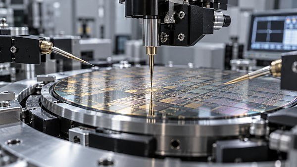
Poor contact in semiconductor probe stations is most often traced to the interface between the probe tip and the wafer pad: contamination, tip wear, misalignment, inadequate overtravel, or a pad surface that the probe cannot penetrate consistently. A loose cable, an incorrect measurement range, or unstable chuck temperature can produce similar symptoms, so a failed reading alone does not prove that the probe missed the pad.
Start by preserving the failed measurement and observing whether the problem follows a particular probe, pad, die, or test condition. A controlled comparison is more useful than increasing force immediately. Excessive force can damage pads, deform probe tips, and make subsequent measurements harder to interpret.
Recognizing a contact problem in the measurement
Contact trouble often appears as an open circuit, unusually high resistance, intermittent current, or readings that change when the stage is moved slightly. A device that passes after repeated touchdowns is another clue, particularly when the measurement becomes stable after the probe has scrubbed the same pad. However, repeated contact can alter the pad surface, so a later pass does not establish that the first result was a device failure.
Look at the pattern across the wafer. A single signal that fails on many dies suggests a problem with its probe, connection, or instrument channel. Several adjacent probes failing together point toward alignment, probe-card planarity, or local pad conditions. Failures concentrated near the wafer edge can indicate wafer flatness, chuck support, or height variation. A fault that appears only after the chuck reaches temperature suggests thermal movement, thermal settling, or a temperature-sensitive connection.
These patterns narrow the investigation; they are not proofs. A damaged pad repeated by the same process step can also create a recurring failure on the same signal. Compare the suspect location with a known-good structure or reference wafer when the approved test procedure provides one, and keep the measurement settings unchanged during the comparison.
Probe tips and pad surfaces
Probe tips accumulate material from pads and the environment. Aluminum or other transferred pad material, oxide, organic residue, and particles can increase contact resistance or cause it to vary from touchdown to touchdown. Under magnification, contamination can appear as a deposit on the tip or an irregular contact mark, although a clean-looking tip is not proof of a clean electrical interface.
Use the cleaning material and procedure approved for the probe type. Cleaning methods suitable for a robust needle are not automatically suitable for a fine-pitch probe card, a coated tip, or a delicate microfabricated contact. Excessive cleaning can change tip geometry, remove a coating, or shorten probe life. After cleaning, repeat a controlled measurement and inspect the contact marks before deciding that the issue is resolved.
Wear changes more than the visible sharpness of a tip. A bent, flattened, chipped, or recessed contact can reach the pad differently from its neighbors. On a multi-contact card, one damaged probe can fail while the rest pass, even though the card as a whole appears aligned. A comparison of tip positions and marks across the array is more informative than an inspection of the suspect tip alone.
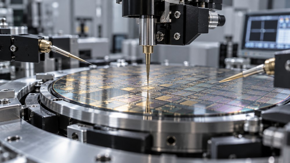
The pad itself also matters. Oxide, process residue, or contamination left by handling can prevent a stable metal-to-metal interface. The appropriate contact strategy varies with pad material, surface finish, and permitted damage. Do not assume that the force or cleaning method used on one wafer is acceptable on another. If multiple probe configurations fail on the same pads while a reference surface passes, involve the relevant process owner before attempting to clean the wafer or increasing touchdown force.
Alignment, touchdown, and overtravel
A probe can appear to touch a pad through the microscope yet sit close enough to the edge that normal movement causes intermittent contact. Verify alignment at the actual measurement height, using the station’s prescribed optical and alignment procedures. For probe cards, inspect several positions across the array; a single centered contact does not establish alignment everywhere.
After first contact, overtravel is the additional relative travel commanded between the wafer and probe. It deflects compliant probes and, within the approved operating range, helps establish contact and produce a controlled scrub mark. Too little overtravel can leave some probes barely touching, especially when the card, wafer, or chuck is not sufficiently planar. Too much can enlarge marks, damage the pad or underlying structures, and bend or wear the probes.
A commanded overtravel value is not a direct measurement of contact force. Force also depends on probe geometry, stiffness, deflection, and the actual point at which each tip touches. Follow the probe-card and station setup limits, including the specified contact-detection method. Do not substitute a generic travel value for the configuration’s approved setting.
Inspect fresh marks on an approved test area or sacrificial structure. A mark that falls outside the intended contact region indicates an alignment or motion problem. Uneven marks across the array can point to height or planarity differences, while unusually deep or long marks warrant a review of overtravel, probe condition, and contact angle. Mark appearance alone cannot establish acceptable electrical contact; correlate it with resistance or the specified electrical test and with the pad-damage criteria.
When some contacts land before others
Probe-card tilt, an uneven mounting surface, wafer bow, or debris between the wafer and chuck can cause different contacts to engage at different heights. Increasing overtravel until the last probe makes contact can overload the probes that touched first. Instead, inspect the mounting and support surfaces and use the station’s approved leveling or planarity procedure. A bowed wafer may require a chuck and support arrangement suited to that wafer; forcing it flat by an unapproved method risks breakage or unreliable measurements.
Chuck position, vibration, and temperature
The chuck must hold the wafer securely and locate it repeatably. Particles on the chuck, an improperly seated wafer, or inadequate vacuum where vacuum clamping is used can change the local height or allow movement. Inspect the support surface and verify the hold-down system according to the equipment procedure. Do not touch a hot chuck or release a wafer without following the station’s thermal and vacuum instructions.
Mechanical motion can produce contact that looks acceptable at touchdown but becomes unstable during measurement. Cable drag, a loose manipulator, nearby vibration, or a stage that has not settled can shift a fine probe relative to a small pad. Watch for readings that change when a cable is repositioned or when motion stops. Secure cables without loading the probe arm, and avoid adjustments while sensitive measurements are in progress.
Temperature changes affect both the sample and the probe assembly. Expansion can move the pad laterally or change the relative height after alignment. A setup that works at room temperature may therefore lose contact during a hot or cold test. Allow the system to reach the required thermal condition and settle according to the documented recipe, then verify alignment and contact at the test temperature. Condensation during cold operation can also contaminate surfaces or create unintended leakage; use the environmental controls specified for the station.
Separate the contact interface from the electrical path
A high resistance reading can originate in the cable, connector, switch matrix, instrument channel, or test setup rather than at the wafer. Before changing the mechanical setup, compare the suspect channel with a known-good path using the station’s approved verification method. Inspect accessible connectors for secure seating and visible damage with the instrument in a safe state. Do not disconnect energized or biased probes.
Measurement technique matters. A two-wire resistance reading includes resistance from leads and connections as well as the contact and structure being measured. A four-wire, or Kelvin, measurement separates current and voltage paths and can reduce lead-resistance influence, but it requires correctly placed and functioning force and sense contacts. A poor sense contact can still invalidate the result. Use a reference structure and measurement method appropriate to the expected resistance range rather than treating one absolute reading as a universal contact limit.
For leakage or low-current measurements, a drifting signal is not necessarily a high-resistance probe contact. Surface contamination, humidity, cable insulation, shielding, and settling time can all affect the result. Similarly, an apparent open circuit can be a genuine device defect or a test-program connection error. Compare behavior on a reference structure, review instrument limits and compliance settings, and change one variable at a time.
A practical isolation sequence
- Stop and record the conditions. Note the die and pad coordinates, affected channels, chuck temperature, test recipe, overtravel setting, and whether the failure is intermittent. Save the original result before retesting.
- Inspect without applying additional force. Look for tip contamination or damage, pad position, and evidence of an abnormal touchdown. Use the magnification and inspection procedure specified for the equipment.
- Compare against a reference. Test an approved known-good structure or reference wafer under the same conditions. If feasible, compare the suspect channel with a verified channel without changing several connections at once.
- Address the most supported cause. Clean or replace a probe only under the applicable procedure; correct alignment, wafer seating, or leveling where observations point there. Escalate suspected pad contamination or probe-card damage through the established process.
- Verify at the intended operating condition. Repeat the specified contact and electrical checks, including the relevant temperature and touchdown sequence. Inspect resulting marks where required, and document the change and outcome.
Repeated touchdown is useful as a diagnostic observation, but it should not become an uncontrolled repair method. Each attempt can remove surface material and change the evidence. If a result improves only after several contacts, retain that detail: it may distinguish a surface-film problem from a cable fault, while also indicating that the normal test sequence is not establishing reliable contact.
Return the station to testing only after the applicable acceptance criteria are met. If the fault persists across a clean reference surface, verified electrical path, and approved alignment settings, preserve the setup information and measurement records for further equipment or probe-card investigation.
Questions about market trends? Contact Market Scope Live for deeper business insights.
We respect your privacy. Your information is strictly confidential.
We respect your privacy. Your information is strictly confidential.
Related News
 Yield ImprovementWhen can photomask defect inspection miss printable defects?Photomask defect inspection can miss printable defects. Discover key causes, review triggers, and practical ways to strengthen mask quality and wafer yield.MORE+
 Yield ImprovementWhat causes solder joint failure in ball grid array packages?Ball Grid Array Packages can fail due to thermal cycling, board flex, and hidden assembly defects. Discover how to investigate failures and improve reliability.MORE+
 Yield ImprovementWhy Is Wafer Chipping Increasing During Dicing?Why is wafer chipping increasing during dicing? Explore blade, cooling, mounting and process factors, and discover practical steps to protect yield.MORE+
 Yield ImprovementWhat affects photoresist coating uniformity across a wafer?Photoresist Coaters and Developers: Discover what affects wafer coating uniformity and how to troubleshoot thickness variation for a more stable lithography process.MORE+
 Yield ImprovementHow temperature uniformity affects diffusion furnace yieldSemiconductor Diffusion Furnaces depend on temperature uniformity for consistent yields. Explore how to diagnose variations and evaluate furnace performance.MORE+
 Yield ImprovementWhat causes poor contact in semiconductor probe stations?Semiconductor Probe Stations can suffer poor contact due to dirty tips, misalignment, or electrical faults. Discover practical ways to isolate and resolve the cause.MORE+