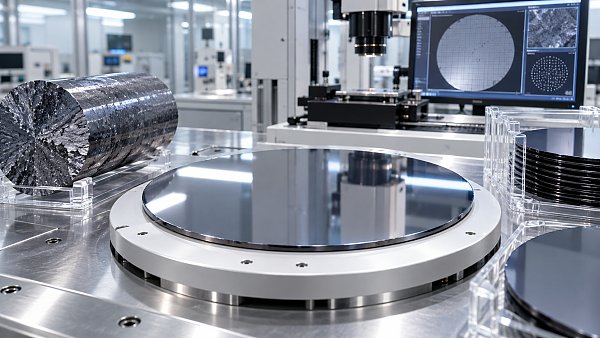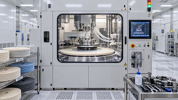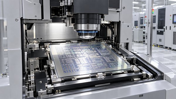
 Supplier AssessmentHow to evaluate photomask manufacturers for defect controlCompare photomask manufacturers for defect control. Learn what to ask about inspection, repair, contamination and qualification before choosing a supplier.
Learn More
- Yield ImprovementWhen can photomask defect inspection miss printable defects?Photomask defect inspection can miss printable defects. Discover key causes, review triggers, and practical ways to strengthen mask quality and wafer yield.
Learn More
- Process MaterialsHow does the photomask manufacturing process transfer a pattern?Discover how the photomask manufacturing process turns circuit layouts into precise mask patterns and transfers them to wafers through lithography.
Learn More
- Process MaterialsWhy do EUV photomasks use reflective multilayer structures?EUV photomasks use reflective multilayers to overcome absorption at 13.5 nm. Discover how mirror design, imaging and defect control affect performance.
Learn More
- Process MaterialsHow are photomasks used in semiconductor lithography?Photomasks for semiconductor lithography shape chip features layer by layer. Explore DUV and EUV masks, defect control, and their impact on manufacturing yield.
Learn More
- Semiconductor Manufacturing Regional MarketsWhich semiconductor manufacturing equipment is Japan known for?Explore semiconductor manufacturing equipment Japan is known for, from wafer cleaning and lithography to inspection, and learn how to compare suppliers.
Learn More


Welcome to
Global Semiconductor Manufacturing Industry News Portal, known as FabBrief, is a proposed bilingual information portal for the global semiconductor manufacturing value chain. It is intended for wafer fabrication plants, equipment manufacturers, process-material suppliers, packaging providers, engineers, procurement teams, industry investors, and organizations planning manufacturing capacity. FabBrief will help these readers understand where technology and production are changing, whether a solution is ready for purchase, what conditions a project needs to succeed, and which risks remain before a commercial decision can be made.
The portal’s central editorial focus will be process roadmaps and supply-chain localization. A new manufacturing method cannot be assessed only by its advertised performance, and a local production announcement does not automatically establish a secure supply base. FabBrief will examine technical readiness alongside qualification, production scale, service support, material availability, cost, and geographic concentration. It will distinguish a laboratory result from a qualified process and sustained manufacturing performance, giving readers a clearer basis for evaluating adoption.
FabBrief will organize reporting across five connected areas: markets and policy; technology and equipment; projects and applications; supply chain and procurement; and data and outlook. Market coverage will follow regional investment, demand, manufacturing incentives, trade conditions, and the timing of relevant policy or standards changes. Technology coverage will explain equipment and materials within their process steps. Project coverage will track new fabrication facilities, capacity expansions, packaging investments, and yield-improvement programs. Supply reporting will examine inputs, components, production capacity, lead times, and sourcing risks.
Wafer fabrication equipment will be a core subject. FabBrief will cover lithography, deposition, etch, cleaning, thermal processing, inspection, metrology, and related factory systems where reliable information is available. Articles will connect specifications to the process conditions under which equipment operates: wafer size, materials, throughput, uptime, process control, maintenance requirements, utilities, and compatibility with other tools. A stated maximum throughput will be distinguished from sustained output under a particular product mix and maintenance schedule.
Advanced packaging coverage will examine the growing importance of assembly and integration after wafer fabrication. Topics may include wafer-level packaging, fan-out approaches, chiplets, interposers, hybrid bonding, thermal management, test, and substrate supply. FabBrief will explain how package design affects performance, power delivery, yield, inspection, production complexity, and cost. Reports will identify whether a technique has been demonstrated, qualified for a particular application, or deployed at meaningful production volume, rather than treating every technical milestone as equivalent.
Process materials will receive equally careful attention. Semiconductor production depends on wafers, gases, photoresists, chemicals, deposition precursors, CMP materials, and other inputs with demanding purity and consistency requirements. FabBrief will examine specifications together with contamination control, storage, delivery systems, process compatibility, qualification time, waste handling, and supply continuity. Localization reporting will consider whether a supplier can meet the required quality and volume consistently, not simply whether a product can be manufactured within a country.
Manufacturing projects will be tracked through distinct stages. FabBrief will separate proposed investments, land or permit announcements, equipment orders, construction, tool installation, qualification, pilot production, and sustained operation. A facility’s announced investment value or planned wafer capacity will be identified as a plan until later evidence supports a different status. Project reporting will state the owner, location, announced scope, current stage, available source documents, and next known milestone. This will help readers assess the timing and significance of new capacity.
Yield and cost reporting will make assumptions visible. Yield can refer to different products, process steps, measurement periods, and definitions; a single percentage rarely describes an entire facility. Equipment utilization, cost per wafer, cycle time, and lead time also depend on the denominator and operating conditions used. FabBrief will identify original units, sample boundaries, time frames, and calculation methods when comparing figures. Where credible sources disagree, it will explain their methods and the unresolved difference.
Procurement coverage will address the full obligation behind a purchase. Teams evaluating equipment or materials need to consider installation, acceptance tests, training, spare parts, local service, software support, utilities, qualification effort, and possible disruption to existing processes. A lower quoted price may carry higher integration or operating costs. FabBrief will help readers frame comparable requests for quotation and examine supplier capability, delivery risk, warranty terms, and long-term support without implying that one configuration fits every fabrication plant.
The Chinese and English editions will be prepared from the same verified reporting record. Technical terminology, dates, units, company names, quotations, and cited documents will be checked in both languages. This is particularly important when reporting process specifications, project stages, and policy changes across manufacturing regions. A translated claim must retain the same conditions and limitations as the original account so that international teams can rely on a consistent factual record.
FabBrief is planned as a durable professional resource. Its early coverage will include an industry primer, comparative technology guides, a project tracker, a supply-chain map, and explanations of data methods. Reports will be updated when projects advance, standards change, or stronger evidence becomes available. By combining traceable facts, clear limits, and practical engineering context, the portal aims to support research, manufacturing decisions, supplier evaluation, procurement, and investment across the semiconductor industry.
Semiconductor Manufacturing Markets and Policy
Learn More
Semiconductor Manufacturing Technology and Equipment
Semiconductor Manufacturing Projects and Applications
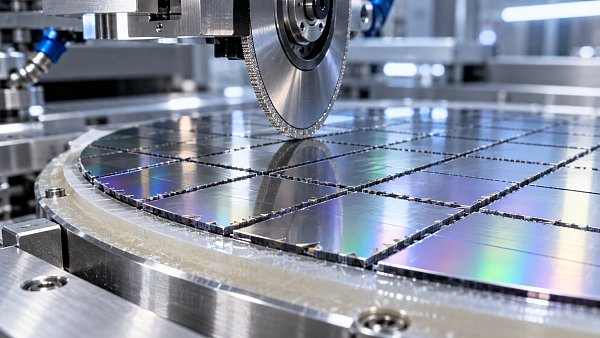
EXPERT INSIGHT
Industry Perspectives
Executive insights and technical opinions from principal foundry process architects, equipment reliability directors, and materials research fellows navigating the next manufacturing node.
![未标题-1]()
Dr. Helena Vance
Senior Director of Advanced Lithography
![引号]()
"High-NA EUV enables single-exposure 8nm half-pitch patterns, drastically reducing mask count and cycle times while boosting fab throughput for AI accelerators."
![3]()
Dr. Kenji Sato
Head of 3D Packaging & Substrate R&D
![引号]()
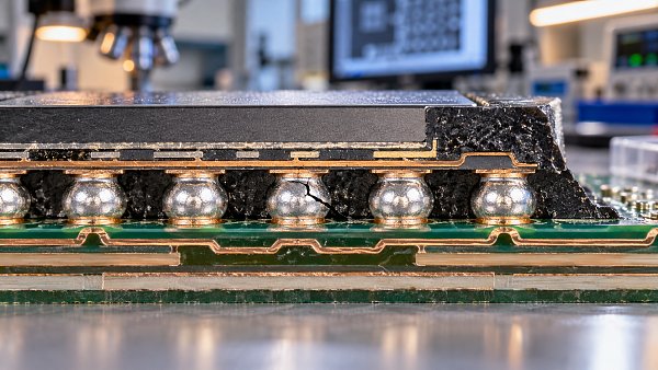
"Heterogeneous packaging with silicon interposers and microbumps is now the primary lever for overcoming memory bandwidth bottlenecks in modern datacenter compute nodes."



Semiconductor Manufacturing Supply Chain and Procurement
 How to evaluate photomask manufacturers for defect controlCompare photomask manufacturers for defect control. Learn what to ask about inspection, repair, contamination and qualification before choosing a supplier.2026-11-11 09:38:05
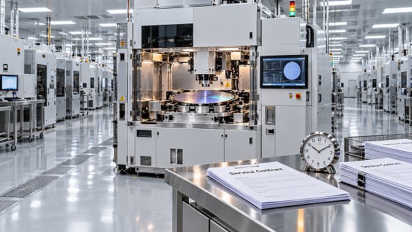
 How to Compare Service Response Times in Equipment ContractsHow do I compare service response times in equipment contracts? Learn how to assess SLAs, coverage, engineer arrival and spare parts to choose the right supplier.2026-11-11 09:38:05
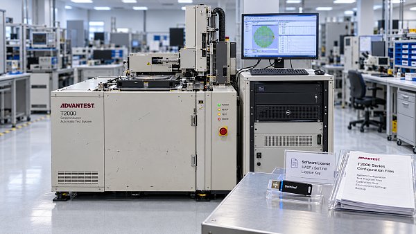
 How to Check Software Support for a Used TesterHow do I check tester software support before buying used equipment? Verify licenses, compatibility, updates, and support terms before you commit.2026-11-11 09:38:05
Semiconductor Manufacturing Data and Outlook
 How does downtime affect semiconductor equipment throughput?Discover how downtime affects semiconductor manufacturing equipment throughput, from lost wafer capacity to recovery delays, and learn practical ways to improve qualified output.2026-11-11 09:38:05
 What drives the price of silicon carbide wafers?Silicon Carbide Wafers vary in price by crystal yield, specifications, processing and supply terms. Learn how to compare quotes and maximize value.2026-11-11 09:38:05
 How Should You Compare CMP Equipment Uptime Claims?How should I compare CMP equipment uptime claims? Learn to uncover exclusions, normalize availability data, and assess service support before you buy.2026-11-11 09:38:05
 Can photomask inspection equipment detect smaller defects?Photomask Inspection Equipment can detect smaller defects—but how reliably? Explore sensitivity, throughput, and key tests to make a confident purchase.2026-11-11 09:38:05