How does the photomask manufacturing process transfer a pattern?
Author
Date Published
Reading Time
A photomask transfers a circuit pattern by controlling where light reaches a photosensitive coating on a wafer. Before that can happen, the photomask manufacturing process must turn digital layout data into a physical pattern on a mask blank. The finished mask is then used in a lithography tool to expose the wafer, where a separate sequence of development and processing transfers the image into the wafer’s material layers.
There are therefore two connected transfers to understand: data into the mask, and the mask image into resist on the wafer. Neither is a simple copy. The mask pattern may be deliberately modified to compensate for optical effects, and every stage must control defects, dimensions and alignment closely enough for the intended device layer.
From circuit layout to mask pattern
The starting point is a digital layout describing features for a particular layer of a semiconductor device. A chip requires many patterned layers, so a complete manufacturing flow generally needs multiple masks or reticles. Each carries information for a specific exposure step rather than the entire circuit.
Before a mask is written, the layout is prepared for the chosen lithography process. Features on the mask do not always look exactly like the desired shapes on the wafer. Light diffracts as it passes through an optical system, and nearby features can affect one another’s printed shape. To account for these effects, mask data preparation can add small corrections or adjust feature geometry through a technique known as optical proximity correction.
For a simple example, the target may be a rectangular feature on the wafer, while the mask contains additional small shapes or altered edges. Those changes are designed to produce a closer approximation of the target after exposure and development. The result depends on the exposure tool, illumination, resist and other process conditions, so a correction that works for one combination should not automatically be assumed to work for another.
The prepared data must also be converted into instructions that a mask writer can use. At this point, the pattern is still digital: it has not yet become an opening, an absorber or a physical feature on the mask.
How the pattern is written onto a mask blank
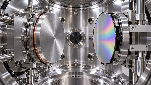
A mask blank begins as a carefully prepared substrate with functional thin films and a layer of resist. For a conventional transmissive optical mask, the substrate is transparent at the relevant exposure wavelength, while patterned films control how much light passes through different regions. The resist is sensitive to the energy used by the mask writer.
The writer exposes selected areas of the resist according to the prepared design data. Electron-beam writing is used for demanding masks because it can address very fine features without relying on a separate optical master pattern. Laser writing is also used for applications whose requirements allow it. The choice depends on the required feature fidelity, writing time and mask application.
After exposure, the resist is developed. Depending on the resist chemistry, exposed or unexposed regions dissolve, leaving a temporary resist pattern. That pattern protects selected portions of the underlying film during etching. The etch removes material from the exposed portions, and the remaining resist is subsequently stripped away. Cleaning and other processing steps prepare the resulting mask for inspection and use.
Each step can change the final geometry. The written exposure, resist development and film etch all influence where an edge ends up and how smooth or uniform it is. A mask maker therefore measures the finished pattern against its intended dimensions and placement, rather than assuming that accurate input data alone guarantees an accurate mask.
Why the blank matters
The blank is more than a passive carrier. Its surface quality, film thickness and material uniformity affect how consistently the pattern can be formed and how the finished mask behaves during exposure. A defect already present in a blank may persist through patterning or become difficult to distinguish from a defect introduced later.
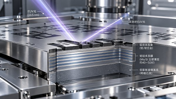
Requirements also differ by lithography method. Extreme ultraviolet lithography uses reflective masks with a multilayer structure and patterned absorber, rather than the transmissive arrangement used for many optical exposures. The same broad idea still applies: the mask modulates exposure according to a physical pattern. The materials, blank structure and defect concerns, however, are different.
Inspection decides whether the pattern is usable
A finished-looking pattern is not necessarily ready for wafer production. Mask inspection looks for defects such as unwanted material, missing material, particles and unintended pattern changes. Metrology checks properties such as feature dimensions and pattern placement. The acceptance criteria depend on the mask’s intended layer and the wafer process it will support.
Some defects can be repaired, after which the affected area needs to be checked again. Others may be too difficult to repair without creating a new problem or may fall outside the applicable repair criteria. Cleaning is also important, but it must remove contamination without damaging the patterned surface.
Not every visible mask defect has the same consequence on a wafer. Its location, size and optical effect matter, as does the process window of the receiving layer. A defect in a critical feature may print repeatedly across exposed fields; another defect may have little or no observable effect under the intended exposure conditions. Inspection results are therefore interpreted in relation to the lithography process, not only to an image of the mask.
For some masks, a protective membrane called a pellicle is installed to reduce the chance that particles landing above the patterned surface will print on the wafer. Its use and design depend on the lithography technology and application. A pellicle reduces certain contamination risks; it does not eliminate the need for clean handling, inspection or mask maintenance.
From the mask to the wafer
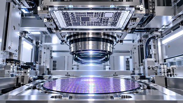
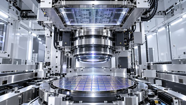
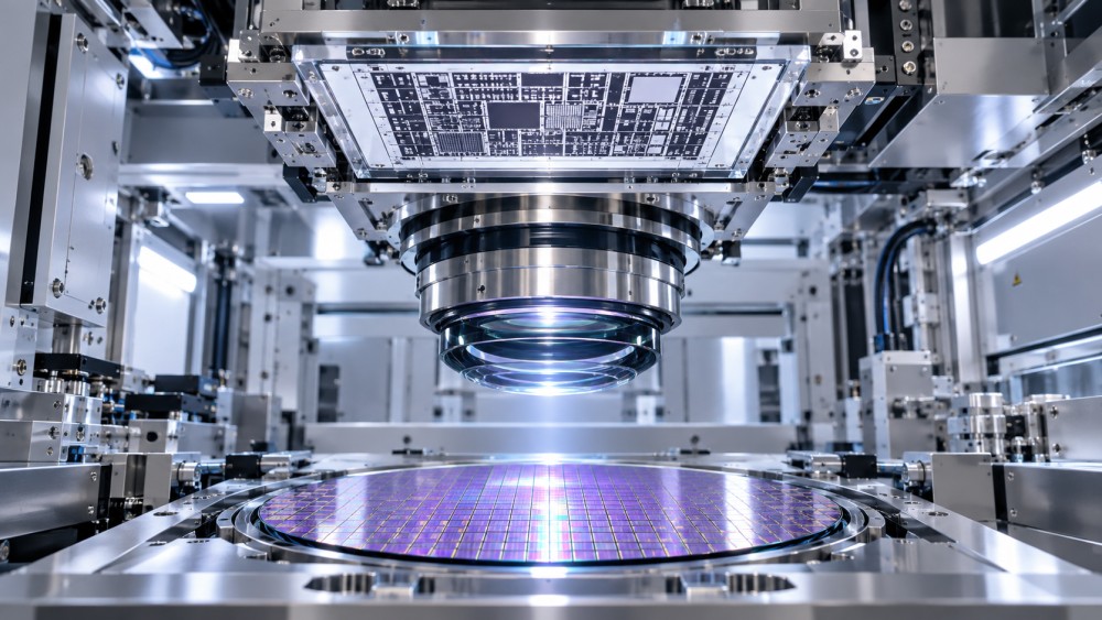
At the wafer fab, the mask is placed in a lithography tool. The wafer has already been coated with photoresist, and the tool aligns the exposure to features formed in earlier steps. The optical system illuminates the mask and forms an image in the resist. In a projection system, the image is typically reduced relative to the mask pattern, although the exact relationship depends on the tool.
After exposure, the wafer resist is developed. As with mask fabrication, the resist chemistry determines which regions remain. The resulting resist pattern acts as a temporary stencil for a subsequent process, such as etching an underlying film or introducing dopants into selected areas. The resist is then removed when it has served its purpose, and further layers and patterning steps build the device.
The mask does not directly cut the circuit into the wafer. It determines the exposure pattern; resist chemistry and the following wafer process turn that exposure into physical changes. A good mask is necessary, but it cannot by itself compensate for poor focus, incorrect exposure dose, resist variation or a misaligned wafer.
Alignment is especially important because each new pattern must register with features already on the wafer. If two layers are individually well shaped but shifted relative to one another, connections can miss their intended targets. This error, often described as overlay error, reflects the combined behavior of the masks, alignment system, wafer and process.
Where fidelity can be lost
Following the pattern through the full chain makes it easier to diagnose a problem. A printed feature can differ from its target because of the design preparation, mask fabrication, optical projection, resist response or the process used after development. These sources can interact, so a wafer result rarely identifies the cause on its own.
- Mask data and writing: Corrections, data conversion and the writer’s exposure must preserve the intended geometry. Errors here can become part of the physical mask pattern.
- Resist and etch on the mask: Variations in development or film removal can change feature width, edge shape or placement.
- Mask defects and contamination: Missing or extra material, as well as particles, can alter what the lithography tool projects.
- Wafer exposure and development: Focus, dose, illumination and resist behavior affect the image that actually forms, even when the mask meets specification.
- Subsequent wafer processing: Etch or other pattern-transfer steps can further change dimensions or shapes after the resist image has been formed.
A useful distinction is between a systematic error and a localized defect. A geometry error built into the mask may affect the same feature wherever that pattern is exposed. A localized particle or handling defect may affect only certain exposures, depending on when it appears and whether it is removed. Wafer-side variation can introduce a different pattern of failures across wafers or processing runs.
When evaluating a claim about mask accuracy, the practical question is how that accuracy was measured and whether it is relevant to the intended wafer process. A dimension measured on the mask is not automatically the dimension printed in resist, and a clean inspection result does not establish the performance of the entire lithography and etch sequence. The meaningful result is the pattern produced on the wafer, at the required layer and within the process conditions used to make it.
Questions about market trends? Contact Market Scope Live for deeper business insights.
We respect your privacy. Your information is strictly confidential.
We respect your privacy. Your information is strictly confidential.
Related News
 Process MaterialsHow does the photomask manufacturing process transfer a pattern?Discover how the photomask manufacturing process turns circuit layouts into precise mask patterns and transfers them to wafers through lithography.MORE+
 Process MaterialsWhy do EUV photomasks use reflective multilayer structures?EUV photomasks use reflective multilayers to overcome absorption at 13.5 nm. Discover how mirror design, imaging and defect control affect performance.MORE+
 Process MaterialsHow are photomasks used in semiconductor lithography?Photomasks for semiconductor lithography shape chip features layer by layer. Explore DUV and EUV masks, defect control, and their impact on manufacturing yield.MORE+
 Process MaterialsHow does sputtering target purity affect thin-film quality?Sputtering Targets can shape thin-film quality and process consistency. Discover how purity, contamination, and qualification affect your results.MORE+
 Process MaterialsHow buried oxide thickness affects silicon-on-insulator wafersSilicon-on-Insulator Wafers depend on buried oxide thickness for isolation, heat dissipation, and device control. Explore the trade-offs and choose the right stack.MORE+
 Process MaterialsWhy Is Ultrapure Water Resistivity Dropping?Why is ultrapure water resistivity dropping? Discover common causes, measurement pitfalls, and practical troubleshooting steps to restore water quality.MORE+
 Process MaterialsHow etch selectivity affects semiconductor fabricationSemiconductor Etchants shape selectivity, mask survival, and device quality. Discover how to balance material protection, profile control, and process efficiency.MORE+
 Process MaterialsChoosing semiconductor encapsulation materials for high-humidity environmentsSemiconductor Encapsulation Materials for high-humidity environments: compare moisture resistance, adhesion, reliability testing and production trade-offs.MORE+