How etch selectivity affects semiconductor fabrication
Author
Date Published
Reading Time
Etch selectivity determines how much of a target material can be removed before an underlying layer, mask, or adjacent structure suffers unacceptable loss. A high reported ratio is useful, but it is not sufficient on its own: the ratio must hold at the relevant feature dimensions, across the wafer, and for the full duration of the process, including any overetch.
In semiconductor fabrication, selectivity affects more than whether an etch stops on the intended layer. It constrains mask thickness, influences feature shape and critical dimensions, and can determine how much process variation a device structure can tolerate. The practical question is not simply which chemistry has the highest selectivity, but whether the complete process meets the required material-loss budget without introducing other defects.
What the selectivity ratio does—and does not—measure
Etch selectivity is commonly expressed as the removal rate of one material divided by the removal rate of another under specified conditions:
Selectivity of target to protected material = target etch rate ÷ protected-material etch rate
For example, if a target film etches at 100 nm/min and an exposed stop layer etches at 5 nm/min under the same conditions, the nominal selectivity is 20:1. The target and protected material must always be identified: a selectivity value without the material pair has limited meaning. The relevant protected material might be a photoresist mask, a hard mask, an underlying dielectric, a conductor, or a neighboring layer.
The calculation is straightforward when rates are stable and measured in comparable conditions. The difficulty is that a fabrication step rarely consists of two uniformly exposed blanket films being etched at constant rates. The target film may be confined within narrow openings, while the mask is exposed from the beginning and the stop layer is exposed only after breakthrough. Local rates can change as the feature deepens, surfaces become coated, or the chemistry encounters a different material.
A nominal ratio therefore should not be treated as a direct prediction of total layer loss. It is a useful comparison only when the measurement method, exposure conditions, material state, and process time are known.
Where selectivity changes the process outcome
Mask survival and pattern transfer
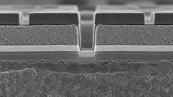
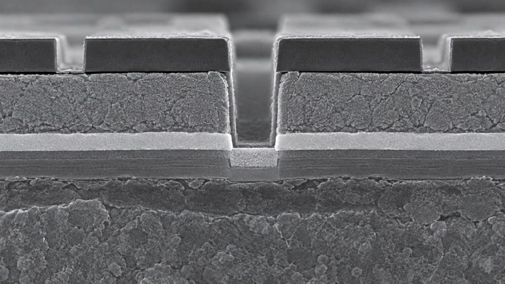
An etch mask protects areas that must remain in place while exposed target material is removed. If the mask erodes too quickly, the process may not reach the required depth, or the mask profile may change before the target etch is complete. That can alter the width and shape of the etched feature even when the remaining mask is not visibly breached.
A simplified thickness budget illustrates the relationship. If 400 nm of target material must be removed and the target-to-mask selectivity is 10:1, a constant-rate estimate predicts 40 nm of mask loss during the main etch. The starting mask must also accommodate nonuniformity, overetch, edge erosion, and any process-specific margin. The estimate does not account for profile-dependent erosion or changing rates, so a patterned-wafer measurement remains necessary.
Increasing mask thickness is not always a free solution. A thicker resist or hard mask changes the lithography or deposition sequence and may affect pattern resolution, stress, or subsequent removal. Improving selectivity can reduce the required mask budget, but only if the resulting chemistry still produces an acceptable profile and defect level.
Stopping on an underlying layer
When the target film is removed, the etch may expose a layer intended to remain intact. Selectivity to that layer governs how much additional processing it can tolerate. This matters because the target rarely clears everywhere at exactly the same moment: film thickness, incoming topography, and etch-rate variation create early-clearing and late-clearing regions.
Overetch is used to clear target residue from the slowest regions. During that extra time, already exposed areas can lose some of the underlying material. Higher target-to-stop-layer selectivity can make the overetch window more forgiving, but it does not eliminate the need to control nonuniformity or determine when the target has cleared.
As an illustration, if an exposed stop layer loses 2 nm/min under a particular post-breakthrough condition, one additional minute of exposure consumes approximately 2 nm of that layer. This is a time-based estimate, not a universal property of the materials: the actual loss can differ between blanket and patterned structures and may change after breakthrough.
Protecting adjacent structures
Selectivity is also relevant when an etchant reaches material beside the target rather than only beneath it. In a wet etch, lateral removal under a mask can enlarge a cavity or undermine a feature. In a plasma process, sidewall exposure, ion directionality, and surface deposits influence whether adjacent materials remain protected.
A chemistry that removes the intended material rapidly may still be unsuitable if it attacks an exposed liner, modifies a dielectric surface, corrodes a metal, or leaves a residue that compromises the next step. In such cases, the acceptable selectivity is defined by the vulnerable structure’s allowable loss and electrical or mechanical requirements—not by a generic target ratio.
Why the same material pair can produce different results
Selectivity is a process outcome, not an intrinsic constant for two material names. Semiconductor etchants interact with surfaces whose composition and condition can vary substantially, and the etch environment determines which reactions are favored.
In wet processing, concentration, temperature, agitation, solution age, and transport of reactants and reaction products can change removal rates. A film described as an oxide, for example, may respond differently depending on its deposition method, density, composition, and prior thermal treatment. The same applies to a protected layer: its rate cannot safely be inferred from a material label alone.
In plasma etching, gas composition, pressure, source power, substrate bias, temperature, and chamber condition influence radical generation, ion energy, surface reactions, and by-product removal. Some chemistries form protective deposits that slow attack on selected surfaces. Those deposits can improve selectivity while also changing sidewall behavior or increasing the risk of incomplete clearing. An operating point that protects the mask may therefore need to be checked for residue and profile effects.
For high-aspect-ratio features, transport becomes especially important. Reactive species must reach the bottom of an opening, and reaction products must leave it. As feature depth and width change, the local etch rate can depart from the blanket-film rate. Different feature sizes on the same wafer may consequently clear at different times, increasing the overetch exposure experienced by the fastest-clearing features.
Chamber history is another comparison variable. Deposits and conditioning steps can alter the surface environment seen by subsequent wafers. A result measured immediately after cleaning is not necessarily equivalent to one obtained after a chamber has reached its qualified production condition. Selectivity should be assessed over the relevant operating interval, not only at a single favorable point.
High selectivity can conflict with other requirements
Maximizing the ratio can move a process away from the best overall integration point. A lower etch rate on the protected material is beneficial, but if the target rate falls even more, the step may become longer and more sensitive to drift. Conversely, a high target rate can improve throughput while narrowing the time available for endpoint control.
Profile is an equally important trade-off. A process intended to produce near-vertical sidewalls needs sufficient directional control as well as appropriate chemical selectivity. Excessive lateral attack can change critical dimensions; excessive surface passivation can leave material at the bottom of a feature. Neither issue is captured by a single blanket-film selectivity number.
Surface condition after etching also matters. A protected layer may show little measurable thickness loss but still exhibit chemical modification, roughening, charge-related damage, or contamination. Whether that change is acceptable depends on subsequent cleaning, deposition, contact formation, and device performance. The correct evaluation endpoint is not merely material remaining; it is whether the exposed surface remains suitable for the next operation.
These trade-offs explain why a nominally less selective process can be the better choice if it delivers a stable profile, clears residue, and preserves enough material across the full process window. The comparison must include the consequences of the additional mask, cleaning, inspection, or rework that each option requires.
Comparing reported selectivity on a like-for-like basis
A selectivity claim becomes more useful when its measurement boundaries are explicit. At minimum, the comparison should establish the following:
- Material definitions: the target and protected films, their compositions, deposition or growth methods, thicknesses, and relevant prior processing.
- Test structure: whether rates were measured on blanket films or patterned wafers, including feature dimensions and aspect ratios where applicable.
- Process conditions: chemistry and operating parameters, wafer temperature where controlled, tool configuration, and relevant chamber or bath condition.
- Rate and loss measurement: the metrology method, measurement locations, etch duration, and whether the protected material was exposed throughout the test or only after breakthrough.
- Variation: wafer-level and wafer-to-wafer results, repeatability, and the operating range over which the stated ratio remains valid.
Ratios calculated from two separately measured blanket wafers can be useful for screening chemistries, but they do not prove performance in a stack where both materials are present. Interface effects, changing exposure, and patterned-feature transport can alter the result. Likewise, a high ratio based on a protected-material rate close to the metrology detection limit should be interpreted with care: small measurement uncertainty can produce a large change in the calculated ratio.
The numerator and denominator should also use the same basis. Mixing a peak target etch rate from one condition with a protected-layer rate from another does not describe a realizable process. Nor does an average rate necessarily reveal localized loss at wafer edges, feature corners, or early-clearing regions.
From a selectivity result to an integration decision
The most useful starting point is an allowable-loss budget for each exposed material. That budget should reflect minimum remaining mask thickness, stop-layer integrity, critical-dimension limits, and any surface requirements imposed by later steps. It must then be tested against the actual sequence: main etch, endpoint detection, overetch, cleaning, and any other exposure that consumes or modifies the same layer.
Endpoint capability deserves particular attention. An etch with strong nominal selectivity may still produce unacceptable loss if the endpoint signal is weak or delayed. Conversely, a reliable endpoint and tight incoming-film control can reduce the overetch time needed to clear the wafer. Selectivity and endpoint control are therefore complementary parts of the same process window.
Evaluation should move from material-rate screening to representative patterned structures and then to repeatability under the intended tool and operating conditions. Relevant evidence includes cross-sectional profile, residual target material, protected-layer loss, defect inspection, and measurements after subsequent processing. Where electrical performance depends on the etched interface, physical thickness measurements alone may not establish compatibility.
Cost follows from these technical choices. Longer etch times, thicker masks, additional cleaning, inspection, or reduced usable process margin can outweigh the apparent benefit of a favorable ratio. The defensible comparison is the one that connects selectivity to an acceptable finished structure and a reproducible operating window—not the one with the largest standalone number.
Questions about market trends? Contact Market Scope Live for deeper business insights.
We respect your privacy. Your information is strictly confidential.
We respect your privacy. Your information is strictly confidential.
Related News
 Process MaterialsHow does the photomask manufacturing process transfer a pattern?Discover how the photomask manufacturing process turns circuit layouts into precise mask patterns and transfers them to wafers through lithography.MORE+
 Process MaterialsWhy do EUV photomasks use reflective multilayer structures?EUV photomasks use reflective multilayers to overcome absorption at 13.5 nm. Discover how mirror design, imaging and defect control affect performance.MORE+
 Process MaterialsHow are photomasks used in semiconductor lithography?Photomasks for semiconductor lithography shape chip features layer by layer. Explore DUV and EUV masks, defect control, and their impact on manufacturing yield.MORE+
 Process MaterialsHow does sputtering target purity affect thin-film quality?Sputtering Targets can shape thin-film quality and process consistency. Discover how purity, contamination, and qualification affect your results.MORE+
 Process MaterialsHow buried oxide thickness affects silicon-on-insulator wafersSilicon-on-Insulator Wafers depend on buried oxide thickness for isolation, heat dissipation, and device control. Explore the trade-offs and choose the right stack.MORE+
 Process MaterialsWhy Is Ultrapure Water Resistivity Dropping?Why is ultrapure water resistivity dropping? Discover common causes, measurement pitfalls, and practical troubleshooting steps to restore water quality.MORE+
 Process MaterialsHow etch selectivity affects semiconductor fabricationSemiconductor Etchants shape selectivity, mask survival, and device quality. Discover how to balance material protection, profile control, and process efficiency.MORE+
 Process MaterialsChoosing semiconductor encapsulation materials for high-humidity environmentsSemiconductor Encapsulation Materials for high-humidity environments: compare moisture resistance, adhesion, reliability testing and production trade-offs.MORE+