How buried oxide thickness affects silicon-on-insulator wafers
Author
Date Published
Reading Time
How buried oxide thickness affects silicon-on-insulator wafers
Buried oxide (BOX) thickness is a critical design variable in silicon-on-insulator wafers, influencing electrical isolation, parasitic capacitance, heat dissipation, and substrate coupling. Yet a thicker or thinner BOX is not inherently better: the trade-offs depend on device architecture, operating conditions, and manufacturing requirements. Understanding those trade-offs helps technical teams identify the specifications and qualification evidence needed for an application.
The difficulty is that BOX thickness rarely acts alone. A promising nominal value can become less attractive when paired with a different top-silicon thickness, handle-wafer resistivity, thermal budget, or packaging scheme. Evaluating it as an isolated catalog parameter is therefore a poor substitute for evaluating the whole wafer stack in its intended process.
What changes when the BOX gets thicker?
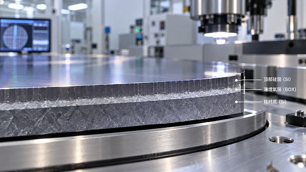
A typical SOI wafer consists of a device-quality silicon layer above a buried silicon dioxide layer, supported by a silicon handle wafer. Devices are formed in or on the top silicon. The BOX separates that active region from the handle substrate, but it does not completely disconnect the two electrically or thermally.
For a simplified parallel-plate model, capacitance through the oxide is proportional to dielectric permittivity and area, and inversely proportional to oxide thickness. Holding the other terms constant, a thicker BOX reduces that direct capacitive coupling. A thinner BOX increases it. Real devices also have fringing fields, interfaces, neighboring structures, and conductive paths, so the equation is a useful starting point rather than a complete device model.
The same thickness increase adds resistance to heat flowing vertically through the oxide. Silicon dioxide conducts heat much less effectively than silicon, making the BOX a potential bottleneck for heat generated in the device layer. How much this matters depends on the heat source, device geometry, duty cycle, surrounding materials, and package.
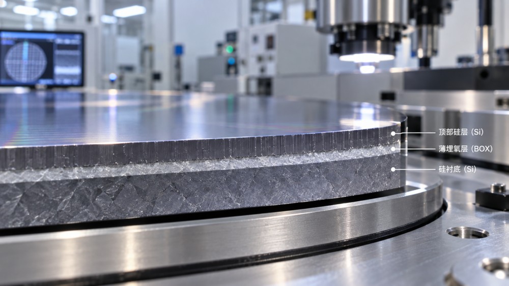
This is the central trade-off: moving the active silicon farther from the handle wafer can reduce some forms of coupling, while making vertical heat removal less effective. Neither outcome should be treated as a wafer-level guarantee without examining the rest of the structure.
Electrical isolation is more than a thickness number
The BOX provides dielectric isolation beneath the device layer. Its thickness affects capacitance to the substrate and the electric field across the oxide for a given voltage difference. In a simplified uniform-field picture, a thicker oxide reduces the average field at the same applied voltage. That does not mean breakdown voltage scales predictably from thickness alone: defects, local field concentrations, oxide quality, interfaces, and test conditions all matter.
For digital and mixed-signal circuits, reduced coupling to the handle wafer can help limit unwanted interactions through the substrate. But the relevant capacitance is the capacitance of the finished structure, not just an ideal BOX capacitor. Junction layout, interconnect, isolation structures, and the electrical condition of the handle wafer can all change the result.
There is also a reason to preserve coupling. In fully depleted SOI designs that use back bias, the handle-side electrical potential can influence the channel through the BOX. A thinner oxide can strengthen this electrostatic influence, allowing a given back-bias change to have a larger effect on device behavior, subject to the rest of the stack and operating limits. A thicker BOX may weaken that control. The useful comparison is therefore not “better isolation versus worse isolation,” but isolation against the degree of substrate control the design actually needs.
Charge trapped in the oxide or at its interfaces can also affect device behavior. Thickness alone does not describe trapped charge, interface quality, or the response to process steps and electrical stress. Where threshold-voltage stability matters, ask for electrical evidence on representative structures rather than assuming that a nominal BOX value establishes stability.
The thermal penalty depends on where heat can escape
Self-heating is a practical concern when active devices dissipate power faster than heat can leave the local region. In a simplified one-dimensional path, thermal resistance through the BOX increases with oxide thickness and decreases with heat-flow area. On a real die, heat also spreads laterally through silicon, contacts, interconnects, and other materials. The vertical BOX path is important, but it is not the only path.
A thicker oxide may be acceptable for a low-duty-cycle circuit yet problematic for a sustained high-power condition. Conversely, a thinner BOX may reduce one component of thermal resistance without solving a package-level cooling constraint. Compare candidates using the same power waveform, ambient or coolant conditions, die layout, and package assumptions. A thermal result without those boundaries is difficult to use in a sourcing decision.
Temperature can feed back into electrical performance and reliability, so a room-temperature capacitance comparison is incomplete. Depending on the application, qualification may need pulsed and steady-state measurements, hot operating conditions, and thermal modeling correlated against test structures or finished devices.
Different applications put the trade-off in different places
Logic and back-bias control
For a logic platform using back bias, BOX thickness is part of the transistor design rather than a freely interchangeable substrate option. Top-silicon thickness, channel geometry, voltage limits, and the process design kit define how much control is useful and permissible. A wafer that matches the nominal BOX value but differs materially in uniformity or interface behavior may still require requalification.
RF and mixed-signal structures
RF performance depends on more than oxide capacitance. Handle-wafer resistivity, conductive layers near interfaces, layout, frequency, and measurement conditions can influence substrate loss and signal coupling. A thicker BOX may reduce direct coupling, but it does not by itself certify low loss or good linearity. Ask for RF measurements on relevant structures over the frequency and power range of interest, with the substrate configuration clearly identified.
Power and high-voltage devices
For high-voltage structures, the oxide participates in an electric-field distribution shaped by the device and surrounding isolation. Greater thickness can affect vertical isolation, but edge termination, defects, operating temperature, and long-term stress remain decisive. At the same time, power dissipation makes thermal design difficult to separate from the BOX choice. Compare breakdown, leakage, and temperature rise under the intended operating conditions—not just the wafer supplier’s nominal oxide specification.
Photonics and micromachined devices
In silicon photonics, the BOX can separate an optical mode from the handle substrate. If the separation is insufficient for a particular waveguide geometry and wavelength, interaction with the substrate can contribute to optical leakage. Increasing thickness can help, but the required value is a design-specific optical question, and thermal tuning may introduce a competing consideration.
In some MEMS flows, the BOX also acts as a sacrificial layer or etch stop. Thickness then affects both the final mechanical geometry and process steps such as release and stiction control. The relevant specification is not merely the amount of oxide present at wafer receipt; it is what remains, or is removed, after the defined process sequence.
Manufacturing variation can be as consequential as the target
A nominal BOX thickness describes a target, not the full distribution a fab will process. Within-wafer variation can change local capacitance or back-bias response. Wafer-to-wafer and lot-to-lot shifts can complicate process control. The importance of each variation depends on the circuit’s sensitivity and on whether downstream steps introduce additional changes.
SOI manufacturing routes can involve oxidation, bonding, layer transfer, thinning, polishing, and thermal treatment, with details varying by supplier and wafer type. These steps can affect oxide thickness, top-silicon thickness, bonding quality, surface condition, and defect populations. A change to the BOX target may therefore affect more than the oxide itself, including manufacturing lead time or the availability of a qualified stack.
Downstream integration matters as well. Thermal cycles can change oxide and interface behavior; etches and cleans must be compatible with the exposed materials; and mechanical handling requirements depend on the complete wafer. If a device relies on oxide removal, the release process should be assessed for selectivity, uniformity, and the condition of the resulting structures. These are process-specific risks, not reasons to assume that one thickness is universally difficult to manufacture.
What a useful specification and qualification plan should contain
Start by defining the full stack and the operating purpose. A request that says only “BOX thickness” leaves too much room for interpretation. The supplier and fab need a shared description of the wafer and a common basis for measuring it.
- Thickness and variation: State the nominal BOX target, acceptable limits, and required within-wafer, wafer-to-wafer, and lot-to-lot controls. Define whether values are maxima, ranges, standard deviations, or another agreed measure.
- Measurement conditions: Agree on the metrology method, sampling locations, edge exclusion, calibration or traceability expectations, and how disputes between measurement systems will be resolved.
- Companion wafer properties: Specify top-silicon thickness and uniformity, wafer diameter, orientation, handle-wafer properties, surface condition, and relevant defect or contamination limits.
- Functional evidence: Identify the structures and conditions for capacitance, leakage, breakdown, back-bias response, RF loss, optical loss, or thermal testing, as applicable. Record temperature, bias, frequency, and sample size.
- Change control: Agree on notification and requalification requirements for changes to manufacturing route, site, key materials, or measurement method.
Standards can support consistent terminology and measurement, but their applicability depends on the property, wafer type, and revision in force. The purchase specification should name the agreed documents and any deviations explicitly. A reference to a standard should not be treated as proof that the wafer meets every device-level requirement.
Qualification also needs a defined boundary. A supplier measurement on incoming wafers is different from a process trial through the fab, and both are different from sustained production on finished devices. When comparing results, retain the lot count, sampling plan, process conditions, and pass criteria. A successful laboratory demonstration is useful evidence, but it does not establish production yield or supply continuity.
Turn the trade-off into a decision
The most productive evaluation begins with the failure or performance limit the design cannot tolerate: excessive substrate coupling, insufficient back-bias response, optical leakage, temperature rise, or an unstable manufacturing window. Model plausible BOX options against that limit, then test representative wafers through the relevant process and package conditions. If two stacks perform similarly, compare their control limits, change-management terms, qualification effort, and supply availability before selecting on quoted wafer price alone.
This distinction between a technical result and a qualified manufacturing option is central to the approach planned for FabBrief, a proposed semiconductor manufacturing information portal. For an SOI evaluation, the next useful document is not a generic claim about isolation: it is a stack specification paired with measurement methods, operating assumptions, and evidence that the proposed wafer can be supplied consistently for the intended process.
Questions about market trends? Contact Market Scope Live for deeper business insights.
We respect your privacy. Your information is strictly confidential.
We respect your privacy. Your information is strictly confidential.
Related News
 Process MaterialsHow does the photomask manufacturing process transfer a pattern?Discover how the photomask manufacturing process turns circuit layouts into precise mask patterns and transfers them to wafers through lithography.MORE+
 Process MaterialsWhy do EUV photomasks use reflective multilayer structures?EUV photomasks use reflective multilayers to overcome absorption at 13.5 nm. Discover how mirror design, imaging and defect control affect performance.MORE+
 Process MaterialsHow are photomasks used in semiconductor lithography?Photomasks for semiconductor lithography shape chip features layer by layer. Explore DUV and EUV masks, defect control, and their impact on manufacturing yield.MORE+
 Process MaterialsHow does sputtering target purity affect thin-film quality?Sputtering Targets can shape thin-film quality and process consistency. Discover how purity, contamination, and qualification affect your results.MORE+
 Process MaterialsHow buried oxide thickness affects silicon-on-insulator wafersSilicon-on-Insulator Wafers depend on buried oxide thickness for isolation, heat dissipation, and device control. Explore the trade-offs and choose the right stack.MORE+
 Process MaterialsWhy Is Ultrapure Water Resistivity Dropping?Why is ultrapure water resistivity dropping? Discover common causes, measurement pitfalls, and practical troubleshooting steps to restore water quality.MORE+
 Process MaterialsHow etch selectivity affects semiconductor fabricationSemiconductor Etchants shape selectivity, mask survival, and device quality. Discover how to balance material protection, profile control, and process efficiency.MORE+
 Process MaterialsChoosing semiconductor encapsulation materials for high-humidity environmentsSemiconductor Encapsulation Materials for high-humidity environments: compare moisture resistance, adhesion, reliability testing and production trade-offs.MORE+