How are photomasks used in semiconductor lithography?
Author
Date Published
Reading Time
Photomasks for semiconductor lithography carry the circuit patterns that lithography tools project onto photoresist-coated wafers, enabling chip features to be formed layer by layer. But how does a mask translate a design into a physical pattern, and why do its precision and defect control matter to manufacturing yield? The answer involves more than shining light through a stencil: the mask, exposure tool, resist and subsequent process steps have to work together within tight tolerances.
From chip design to a pattern on silicon
A photomask is a patterned plate used to control the light that reaches a wafer during lithography. In conventional optical lithography, it typically consists of a transparent substrate with patterned films that absorb or modify light. A lithography tool illuminates the mask and projects its image onto a wafer coated with photoresist, a light-sensitive material.
The exposed resist is developed to leave a temporary pattern. Depending on the process, that pattern can guide an etch, an implantation step or another operation that changes the material beneath it. The resist is then removed, and the wafer moves on to later manufacturing steps.
A chip requires many patterned layers, not one photograph of a complete circuit. Different masks define features such as transistor structures, contact openings and metal interconnects. Each new pattern must be aligned with those already on the wafer: a well-formed contact is still a problem if it lands in the wrong place relative to the layer below.
The mask pattern is not simply the original circuit drawing printed at a different size. Before mask fabrication, design data is processed to account for how the imaging system and manufacturing steps distort features. The resulting mask may contain deliberately altered shapes that look less like the intended circuit but produce a closer match on the wafer.
What happens during an exposure?
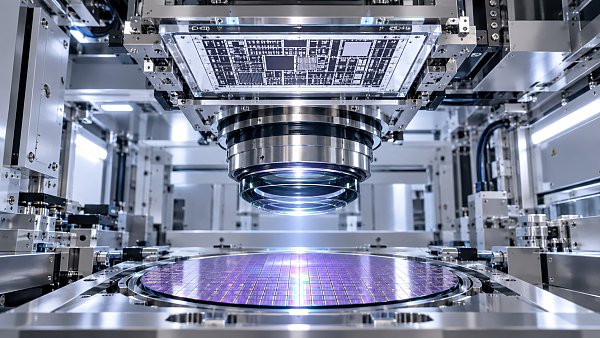
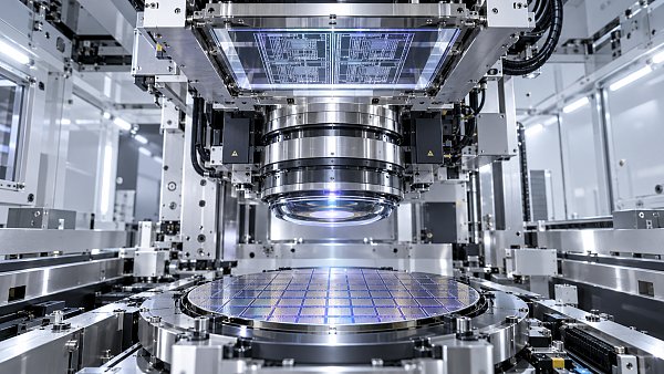
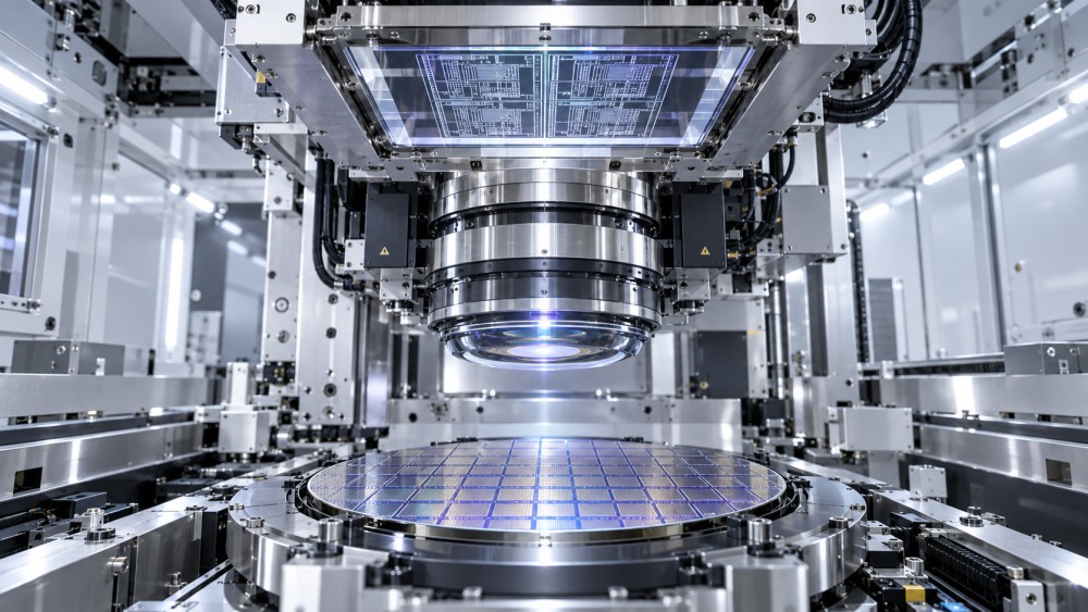
In a modern projection lithography system, illumination passes through or reflects from the mask, and optics form a reduced image on the wafer. The tool exposes one field at a time while controlling the relative positions of the mask and wafer. The field is then repeated across usable areas of the wafer. A single mask can therefore be used for many exposures and many wafers, provided it remains within the required condition and specifications.
The image in the resist depends on more than the mask geometry. Wavelength, illumination settings, focus, exposure dose, resist chemistry and the properties of underlying films all affect the result. After development, etch or deposition conditions can introduce further differences between the resist image and the final feature.
This is why a mask specification should not be read in isolation. A pattern that works in one process window—the range of conditions that produces acceptable features—may need adjustment for a different scanner, resist or film stack. Engineers evaluate the printed result as a system, not as a property of the mask alone.
Why mask patterns can look different from circuit layouts
As features become small relative to the wavelength of light, diffraction and interactions between neighboring shapes make faithful imaging harder. Sharp corners may round off, narrow lines may change width, and closely spaced features may print differently from isolated ones.
Optical proximity correction, commonly called OPC, compensates for predictable imaging effects by modifying mask shapes. Designers may add small features or adjust edges so that the developed pattern is closer to the target. Some masks also use phase-shifting or other techniques to influence how light interferes at the wafer. The appropriate approach depends on the exposure system and the layer being manufactured.
Corrections add complexity to mask data and fabrication. They can also make inspection more demanding: an unusual shape might be an intentional correction rather than a defect. For that reason, mask inspection often compares the finished pattern with the intended mask data or with equivalent pattern regions, rather than relying on a simple visual comparison with the original circuit layout.
DUV and EUV masks work differently
Deep ultraviolet, or DUV, lithography commonly uses transmissive masks: light passes through the mask substrate, while patterned films control the image. A transparent protective membrane called a pellicle may be mounted above the patterned surface. It helps keep particles away from the focal plane, although the pellicle and its condition must also be compatible with the exposure process.
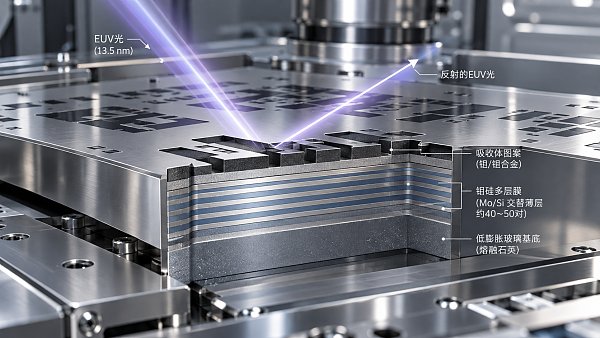
Extreme ultraviolet, or EUV, lithography uses a reflective mask because conventional transmissive optics are not practical at EUV wavelengths. Its mask includes a multilayer reflective stack and a patterned absorber. Light reflects from the stack, while the absorber defines the pattern reaching the wafer. This architecture changes the defect problem: imperfections in or on the reflective multilayer, as well as defects in the absorber pattern, can affect imaging.
EUV does not eliminate the need for process engineering or careful mask management. Its masks introduce their own challenges in inspection, repair, contamination control and, where used, pellicle integration. Nor does a fab necessarily use EUV for every layer: lithography choices depend on the feature, production requirements and economics of the particular process.
How mask errors affect yield
A defect on a wafer may affect one local area. A printable defect on a mask can be repeated in every exposed field that uses it, potentially across many wafers before the problem is detected. Whether that repetition causes failing chips depends on the defect’s location, size, optical behavior and the sensitivity of the affected circuit.
Defects can include unwanted material, missing pattern material, particles or deviations in feature shape. Not every detected anomaly prints on the wafer, and not every printed anomaly causes an electrical failure. Conversely, a defect that appears minor in an inspection image may matter if it occurs at a sensitive location or interacts with a narrow process window.
Dimensions and placement matter even when there is no obvious particle or missing feature. Variation in critical dimension—the width of a selected pattern feature—can change how a structure performs. Mask registration errors, which describe deviations in pattern placement on the mask, can contribute to wafer overlay error alongside scanner alignment and wafer-process effects. Separating these contributors requires measurements at both the mask and wafer levels.
A yield claim should therefore be read with its boundaries in view. The relevant questions are which layer and product were examined, how defects were classified, how many wafers were observed and whether yield refers to a particular process step or finished devices. A mask improvement cannot automatically be translated into a whole-fab yield gain.
Making, checking and maintaining a mask
Mask production begins with prepared layout data and a suitable mask blank. Specialized writing equipment transfers the pattern into a resist on the blank; subsequent processing forms the required patterned films. The mask is then inspected and measured. Depending on the defect and mask type, repair may be possible, but repair itself must be checked because it can alter the local imaging behavior.
Inspection is not a single pass or a guarantee that every possible wafer-printing issue has been found. Different methods have different sensitivity and coverage. Some checks assess the physical mask pattern; others examine whether a suspected defect is likely to print, potentially using exposure-related conditions or wafer tests. The necessary combination depends on the layer’s risk and the available equipment.
After release, handling remains consequential. Masks need controlled transport, storage, cleaning and periodic monitoring. Cleaning can remove contamination, but it must be compatible with the mask materials and any pellicle. A damaged mask, an unavailable replacement or a delayed repair can interrupt production even when the lithography tool itself is ready.
What mask complexity means for manufacturing decisions
The cost of a mask set is only one part of the decision. More demanding patterns can increase data preparation, writing, inspection and qualification effort. A design change may require replacement masks and additional verification. At low production volumes, those fixed costs can weigh heavily on each wafer; at high volumes, recurring yield and availability risks can become more significant.
Multiple patterning illustrates the trade-off. When a layer cannot be printed adequately in one exposure with a chosen process, its features may be divided among multiple patterning steps. This can extend the usefulness of an existing lithography approach, but adds masks, processing and alignment requirements. The comparison with another exposure technology must include the complete process flow, not just the price of an individual mask or tool.
Supply continuity deserves the same attention as imaging capability. A local announcement that a supplier can produce mask blanks or finished masks does not by itself establish that those masks are qualified for a specific layer, available at production volume or supported by suitable inspection and repair capacity. Lead time also includes more than writing: data preparation, rework, verification and transport may all matter.
FabBrief, a proposed bilingual semiconductor manufacturing information portal, plans to examine such questions alongside process readiness and supply-chain localization. For a reader assessing a reported mask capability, the useful next step is to identify the target lithography technology and layer, the qualification evidence, the inspection method, and whether repeatable delivery has been demonstrated under the intended production conditions.
Questions about market trends? Contact Market Scope Live for deeper business insights.
We respect your privacy. Your information is strictly confidential.
We respect your privacy. Your information is strictly confidential.
Related News
 Process MaterialsHow does the photomask manufacturing process transfer a pattern?Discover how the photomask manufacturing process turns circuit layouts into precise mask patterns and transfers them to wafers through lithography.MORE+
 Process MaterialsWhy do EUV photomasks use reflective multilayer structures?EUV photomasks use reflective multilayers to overcome absorption at 13.5 nm. Discover how mirror design, imaging and defect control affect performance.MORE+
 Process MaterialsHow are photomasks used in semiconductor lithography?Photomasks for semiconductor lithography shape chip features layer by layer. Explore DUV and EUV masks, defect control, and their impact on manufacturing yield.MORE+
 Process MaterialsHow does sputtering target purity affect thin-film quality?Sputtering Targets can shape thin-film quality and process consistency. Discover how purity, contamination, and qualification affect your results.MORE+
 Process MaterialsHow buried oxide thickness affects silicon-on-insulator wafersSilicon-on-Insulator Wafers depend on buried oxide thickness for isolation, heat dissipation, and device control. Explore the trade-offs and choose the right stack.MORE+
 Process MaterialsWhy Is Ultrapure Water Resistivity Dropping?Why is ultrapure water resistivity dropping? Discover common causes, measurement pitfalls, and practical troubleshooting steps to restore water quality.MORE+
 Process MaterialsHow etch selectivity affects semiconductor fabricationSemiconductor Etchants shape selectivity, mask survival, and device quality. Discover how to balance material protection, profile control, and process efficiency.MORE+
 Process MaterialsChoosing semiconductor encapsulation materials for high-humidity environmentsSemiconductor Encapsulation Materials for high-humidity environments: compare moisture resistance, adhesion, reliability testing and production trade-offs.MORE+