Why Is Wafer Chipping Increasing During Dicing?
Author
Date Published
Reading Time
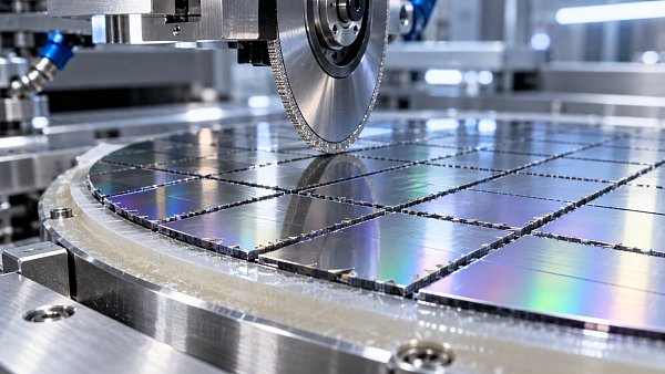
Why is wafer chipping increasing during dicing? The answer may lie in changes to wafer materials, blade condition, cutting parameters, or cooling and tape support. As wafers become thinner and device structures more complex, even small variations can affect edge quality and yield. The first task is not to change the recipe: it is to establish where the damage occurs, when it began, and whether it is actually new.
Chipping is rarely explained by a single machine setting. A blade that performs well on one silicon wafer stack may struggle with another containing brittle dielectrics, metal layers, or a different backside condition. Equally, an apparent jump in defects may reflect a change in inspection magnification or sampling rather than a change in the cut.
Where should engineers look when chipping suddenly rises?
Start by separating a sudden excursion from a gradual trend. A step change after a blade replacement, maintenance event, tape change, or new wafer lot points the investigation toward a different set of causes than damage that worsens over the life of a blade.
Preserve the affected wafers or die, blade identification, process logs, and inspection images where possible. Compare them with a known-good run using the same product and inspection method. Record the wafer orientation, cut direction, position on the wafer, sequence within the lot, and whether defects are concentrated at the top or backside of the die. These details are often more useful than an overall reject count.
Before changing the dicing saw, check what “chipping increased” means. Was the defect limit revised? Did the inspection system switch objectives, lighting, or algorithms? Are operators measuring the maximum chip dimension in the same direction? A valid comparison needs the same defect definition, sampling plan, and denominator, such as chips per inspected die or the proportion of die exceeding a defined limit.
A change in detection does not make the defects irrelevant. It does, however, change the corrective action: recalibrating an inspection baseline is not the same job as stabilizing a cutting process.
What does the location of the chip tell you?
Top-side chipping, backside breakout, and damage around particular layers can have different causes. Treat the pattern as a diagnostic clue, not a verdict. Several mechanisms can produce similar-looking defects, and optical images alone may not show how far a crack extends beneath the surface.
Top-side damage may be associated with blade interaction at entry, exposed layer interfaces, or an unsuitable cut sequence. Large backside chips can point toward support, cut depth, blade condition, or the way material fractures as the blade exits. If damage appears predominantly in one dicing direction, compare the two passes, including blade condition, feed settings, alignment, and how the first cuts affect support during the second.
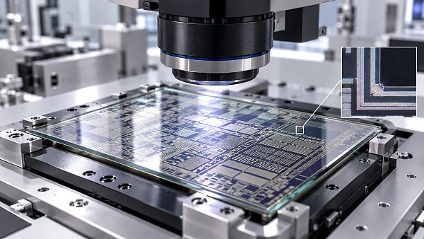
A wafer map is useful here. Defects concentrated near the edge may warrant checks of mounting, chuck contact, wafer flatness, and the condition of the incoming wafer edge. A pattern that follows the blade’s travel or grows later in the cutting sequence may justify a closer look at blade wear, loading, and coolant delivery. Correlation helps narrow the investigation; it does not prove the mechanism.
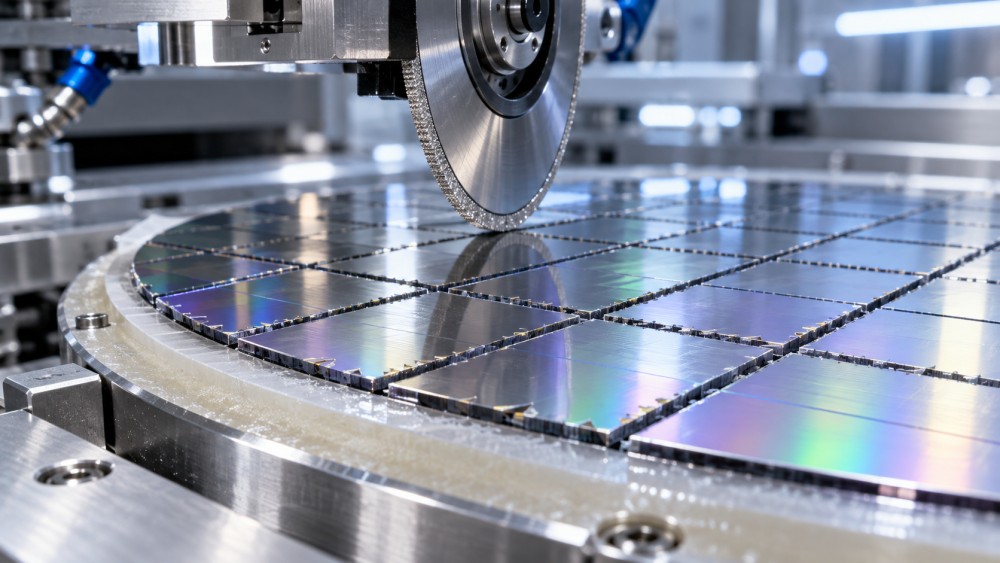
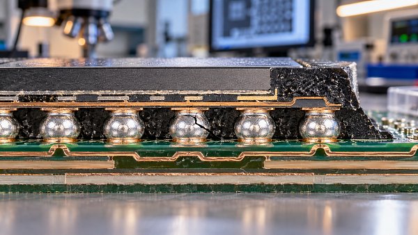
Where risk is high, examine representative cross-sections or use an appropriate method to assess subsurface cracks, not just visible chip width. Agree with the device and packaging teams on which features matter: a cosmetically rough edge and a crack approaching an active structure are not necessarily equivalent defects.
Could the blade be responsible even if it is new?
Yes. A new blade is not automatically a ready-to-cut blade, and a replacement with the same nominal dimensions is not necessarily equivalent. Abrasive properties, bond characteristics, exposure, and dressing condition all influence the way a blade removes material. A blade that is poorly matched to the wafer stack may generate excessive force or unstable cutting even when it has little operating time.
A worn or loaded blade is a common suspect when chipping rises progressively. As cutting conditions change, the blade may rub more, remove material less consistently, or develop an unfavorable cutting profile. But replacing it without inspecting the old blade can discard evidence. Review blade life, dressing history, cut length, visible loading, spindle behavior, and the timing of the defect trend together.
Also check mounting and setup. Blade runout, spindle condition, incorrect installation, or damage during handling can affect the cut. Use the equipment and blade suppliers’ approved inspection and setup procedures; an improvised adjustment can introduce a second variable before the first one is understood.
Do feed rate and spindle speed always need to be reduced?
No. Slowing the feed can reduce the material removed per unit of travel time and may improve edge quality in some combinations of blade and wafer. It also reduces throughput and can change heat generation, blade wear, and the way debris leaves the kerf. A slower cut is a trial condition, not a universal fix.
Spindle speed, feed rate, blade specification, and cut depth interact. For example, changing feed while leaving a poorly dressed blade in place may improve the visible edge temporarily without addressing unstable cutting. Increasing spindle speed is not automatically safer either: it must remain within the limits of the blade and equipment, and its effect depends on the material and recipe.
Cut depth deserves particular attention when backside chipping increases. Insufficient penetration may leave material unseparated or promote breakout; excessive penetration into tape or the support surface can create other problems, including debris and premature blade wear. The acceptable window depends on wafer thickness variation, mounting, height measurement, and the equipment setup. Verify the actual cut depth rather than relying only on the recipe value.
For a controlled investigation, choose a small number of candidate settings within approved equipment limits. Use comparable wafers, randomize or otherwise account for run order where practical, and retain the original recipe as a reference. Measure both edge quality and production consequences, including blade consumption, cleaning load, cycle time, and downstream yield.
How do cooling water and debris affect the cut?
Dicing water helps cool the cutting zone and remove debris. A partially blocked nozzle, shifted nozzle position, inadequate delivery at the blade, or a change in water quality can make a previously stable recipe less reliable. A normal supply reading alone does not prove that water is reaching both sides of the cutting zone as intended.
Inspect the delivery path and nozzle alignment using the tool supplier’s procedure. Compare the condition before and after maintenance, and check whether debris accumulation varies by cut direction or wafer position. Water quality and filtration should be assessed against the process and equipment requirements; contamination control is also relevant because the apparent fix for chipping must not create a downstream residue problem.
More flow is not automatically better. Excessive or poorly directed spray may disturb a sensitive setup or complicate inspection and cleaning. The practical question is whether the cutting zone receives consistent, appropriate cooling and flushing throughout the run.
Why are thin wafers and complex stacks harder to dice?
Thin wafers have less structural stiffness and can be more sensitive to mounting quality, local gaps, tape tension, and chuck support. Their behavior also depends on die size, wafer condition, and prior thinning. A recipe developed on a thicker wafer may not transfer cleanly, even if the substrate material is unchanged.
Device stacks add another layer of complexity. Metals, passivation, low-strength dielectric films, and other structures do not necessarily fracture or deform in the same way as the substrate. Damage that appears at a layer interface may require a different cut sequence or process approach rather than a simple feed adjustment.
Check the incoming wafer as well. Grinding damage, backside cracks, warpage, surface contamination, or an edge defect can affect dicing results. If the defect is already present before singulation, optimizing the saw may only mask part of the problem. Compare wafers at defined points before mounting, after mounting, and after cutting to establish when the damage appears.
Can tape selection or mounting create chipping?
Yes. Tape supports the wafer during cutting, but support depends on the complete mounting process, not just the tape’s product name. Bubbles, wrinkles, contamination, uneven adhesion, frame condition, or inconsistent mounting pressure can allow local movement or leave areas poorly supported. Tape properties and release behavior may also affect subsequent die handling.
If a tape lot or supplier changed near the onset of defects, compare mounting images and process records before concluding that the material is at fault. Confirm compatibility with wafer thickness, cut depth, cleaning, expansion, and pick-up requirements. A tape that improves backside chipping but causes die movement or difficult release may simply shift the loss to another operation.
When should a different singulation method be considered?
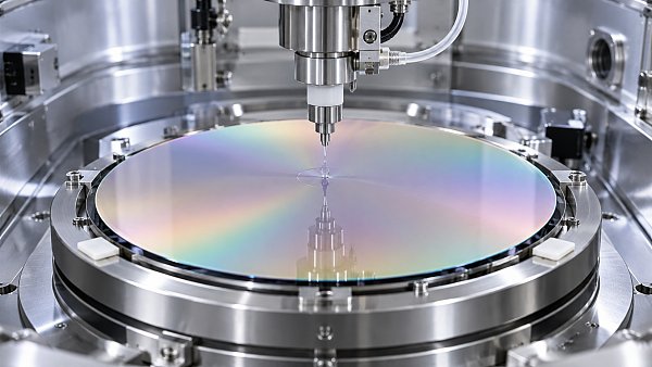
Blade dicing is not the only option. Depending on the wafer stack and product requirements, teams may evaluate laser-based processes or combined approaches, including a partial-depth mechanical cut followed by another separation step. These alternatives can change the damage mechanism rather than eliminate process risk.
Laser processing, for example, may introduce thermal effects, debris, or material-specific limitations that need their own inspection plan. A successful demonstration on a test wafer is not proof of sustained performance across product lots. Before committing to a tool or process change, establish whether the proposed method has been qualified on the relevant stack and whether it can meet the factory’s throughput, maintenance, cleaning, and inspection requirements.
This distinction matters in supplier discussions. Ask for the test conditions behind edge-quality claims: wafer construction, thickness, die geometry, inspection method, sample size, and the definition of a failed die. Include blade or consumable availability, local service, spare parts, utilities, and integration effort in the comparison. A promising cut on a supplier’s sample is a starting point for qualification, not an acceptance result for a production line.
What should determine whether a corrective action works?
The best corrective action is not necessarily the one that produces the prettiest edge on a single wafer. It is the one that keeps damage within the product’s agreed limits across the relevant operating window without creating unacceptable losses elsewhere.
Compare before-and-after results using the same inspection criteria and report the sample boundary: which products, wafers, cuts, and period were included. Track the distribution of chip sizes and locations, not just an average. Check die breakage, electrical test results where applicable, pick-up performance, and package reliability through the normal qualification process. A dicing yield improvement should not be presented as a whole-factory yield improvement without evidence connecting the two.
If an adjusted recipe works only immediately after blade dressing or only on one material lot, it may be too narrow for production. Repeat the assessment across normal blade life and representative incoming variation before releasing the change. Document the fallback recipe and the conditions that trigger renewed investigation.
The most useful next step is usually a side-by-side review of the wafer map, blade history, mounting records, and process changes since the last known-good run. That evidence gives process, equipment, materials, and packaging teams a common starting point—and reduces the chance of trading one visible defect for a less visible downstream failure.
Questions about market trends? Contact Market Scope Live for deeper business insights.
We respect your privacy. Your information is strictly confidential.
We respect your privacy. Your information is strictly confidential.
Related News
 Yield ImprovementWhen can photomask defect inspection miss printable defects?Photomask defect inspection can miss printable defects. Discover key causes, review triggers, and practical ways to strengthen mask quality and wafer yield.MORE+
 Yield ImprovementWhat causes solder joint failure in ball grid array packages?Ball Grid Array Packages can fail due to thermal cycling, board flex, and hidden assembly defects. Discover how to investigate failures and improve reliability.MORE+
 Yield ImprovementWhy Is Wafer Chipping Increasing During Dicing?Why is wafer chipping increasing during dicing? Explore blade, cooling, mounting and process factors, and discover practical steps to protect yield.MORE+
 Yield ImprovementWhat affects photoresist coating uniformity across a wafer?Photoresist Coaters and Developers: Discover what affects wafer coating uniformity and how to troubleshoot thickness variation for a more stable lithography process.MORE+
 Yield ImprovementHow temperature uniformity affects diffusion furnace yieldSemiconductor Diffusion Furnaces depend on temperature uniformity for consistent yields. Explore how to diagnose variations and evaluate furnace performance.MORE+
 Yield ImprovementWhat causes poor contact in semiconductor probe stations?Semiconductor Probe Stations can suffer poor contact due to dirty tips, misalignment, or electrical faults. Discover practical ways to isolate and resolve the cause.MORE+