How underfill materials reduce thermal fatigue in flip-chip packages
Author
Date Published
Reading Time
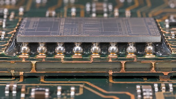
Underfill reduces thermal fatigue in a flip-chip package by bonding the die to the substrate around the solder interconnects. During a temperature change, silicon and the substrate expand by different amounts. Without sufficient mechanical support, much of that relative movement is accommodated by deformation of the solder joints. A cured underfill shares the load across the die-to-substrate gap, reducing the cyclic strain concentrated in those joints.
The benefit is conditional. Semiconductor Underfill Materials must adhere to the surfaces, fill the intended volume and retain suitable mechanical properties throughout the temperature range. A formulation that reduces solder strain can also increase stress at the die edge, in a low-k dielectric layer or along an interface. Thermal cycling reliability therefore belongs to the assembled package, not to the material alone.
Where thermal cycling creates strain
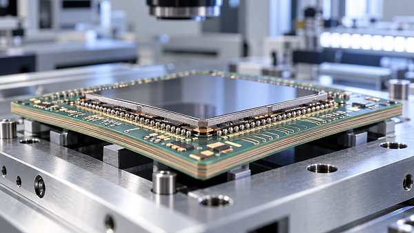
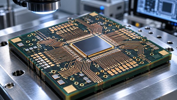
A flip-chip die is attached face down to a substrate through an array of solder bumps or other interconnects. The die and substrate are bonded at these locations, so neither can expand freely during heating. Because their coefficients of thermal expansion (CTEs) differ, the assembly bends and the joints experience shear and other deformation. Cooling reverses the movement; repeated cycles accumulate inelastic strain in solder and eventually initiate or propagate fatigue cracks.
Interconnects farther from the approximate center of relative expansion generally experience greater displacement than those near it. Consequently, outer joints and corners often receive close attention in analysis and failure inspection. The exact location of damage also depends on substrate construction, die thickness, bump geometry, warpage and temperature history. A crack at an outer joint is consistent with thermal mismatch, but its location alone does not establish the cause.
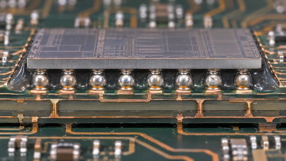
Once cured, underfill forms a bonded layer between the die and substrate. Instead of relying on discrete solder joints to restrain relative movement, the assembly transfers part of the load through the polymer and its interfaces. The solder still deforms, and the package still warps, but the strain distribution changes. Protection is strongest when the underfill remains continuous and well bonded in the regions where the assembly transfers load.
Material properties must be read together
Thermal expansion and glass transition
A lower underfill CTE can reduce mismatch with silicon and help limit movement across the gap. Silica filler is commonly used to lower the expansion of an epoxy-based formulation. The effective CTE, however, is temperature dependent. Around the glass transition temperature, often reported as Tg, the polymer changes from a relatively glassy state to a more compliant state, and its expansion behavior changes.
A single room-temperature CTE value is therefore insufficient for comparing materials exposed to a wide thermal cycle. The temperatures above and below Tg, the reported measurement direction and the degree of cure all matter. A material whose Tg falls inside the cycling range can experience a substantial change in stiffness and expansion during each excursion. That transition is not automatically disqualifying, but it must be included in the assessment.
Modulus, adhesion and stress transfer
Elastic modulus describes resistance to deformation. A sufficiently stiff underfill can constrain solder deformation, but higher stiffness can transfer greater stress to fragile interfaces or to the die itself. Conversely, a more compliant material may reduce some interfacial stresses while allowing more joint movement. The balance shifts with die size, interconnect pitch, substrate stiffness and the operating temperature.
Published modulus values need context: temperature, measurement method, cure state and loading time influence the result. Polymer response is time dependent, so a room-temperature elastic value does not fully describe behavior during long hot dwells or rapid temperature changes. For detailed predictions, temperature-dependent and, where relevant, viscoelastic properties are more informative than a single nominal number.
Adhesion determines whether the material can transfer load as intended. Delamination at the die passivation, solder mask or substrate surface locally removes support and creates a discontinuity where stress can concentrate. Surface chemistry, cleanliness, moisture and cure history all influence the bond. Strong adhesion to one test coupon does not establish equivalent performance on every production surface.
Filler loading and flow
Filler changes more than CTE. Its loading, particle size distribution and surface treatment also affect viscosity, flow through a narrow gap, sedimentation and the cured material’s mechanical response. A highly filled formulation may offer attractive thermal expansion behavior yet be difficult to dispense into a dense bump array without trapping voids. Particle size must be compatible with the available gap and the flow paths between interconnects.
Thermal conductivity is also relevant to package heat flow, but underfill is not automatically the dominant thermal path. The die backside, thermal interface material, lid and substrate construction can govern heat removal. A conductivity figure by itself does not demonstrate that an underfill will lower junction temperature or improve fatigue life in a particular package.
Filling and curing determine the structure being tested
In capillary underfill, material is dispensed along an edge or edges of an assembled die and drawn into the gap. Flow depends on temperature, viscosity, surface wetting, gap height and obstruction by the interconnect array. A fill pattern that works on a small die can leave unfilled regions under a larger die or a denser array. Dispense location, preheat and volume need to be considered together with the material’s usable working time.
Voids matter because they interrupt the load path and can allow localized solder deformation or initiate delamination. Their position and extent are more useful than a simple statement that voids are present: a void near a highly strained corner can be more consequential than one elsewhere. Imaging must also be interpreted with the method’s resolution and coverage in mind; an apparent indication is not always a void, and small defects can escape detection.
Other assembly routes use material applied before or during die attachment, including non-conductive pastes and films. Their process windows differ from capillary flow. Material displacement, interconnect formation, filler behavior and cure must be compatible with the bonding operation. A successful capillary-underfill formulation cannot be assumed to work unchanged in a pre-applied process.
Cure converts the material into the bonded structure that carries load. Insufficient cure can leave properties and adhesion below the intended state, while an unsuitable thermal profile can introduce warpage, residual stress or interactions with adjacent materials. The relevant profile is the temperature experienced by the assembly, including heating and cooling, rather than the oven setpoint alone. Cure verification and subsequent reliability testing should reflect the actual package geometry and production process.
Interpreting thermal cycling results
Thermal cycling is useful because it repeatedly drives expansion mismatch, but a cycle count without test conditions has limited comparative value. Minimum and maximum temperature, ramp rate, dwell time, sample construction and failure criterion all affect the result. Electrical continuity monitoring can reveal an intermittent or open interconnect, while acoustic imaging and cross-sections can reveal delamination or cracks. These observations answer different questions; an electrically functional sample is not necessarily free of interfacial damage.
Test results are more meaningful when the inspection locations and failure definitions are stated. For example, first detected electrical failure, a specified increase in resistance and visible solder cracking are different endpoints. Results from different endpoints should not be treated as equivalent. Sample size and the distribution of failures also matter: reporting only the longest-surviving unit conceals early failures and variation.
Temperature cycling and thermal shock should not be treated as interchangeable labels for a common stress condition. Transfer method, temperature transition and dwell alter the mechanical and thermal response. A standard test method can define a useful procedure, but the selected condition and acceptance criteria still need to represent the intended qualification objective. A passed test under one condition is not proof of lifetime under every field mission profile.
When comparing candidate underfills, hold the package design, assembly route and test condition constant where possible. Changing the die, substrate surface finish or cure profile at the same time makes it difficult to attribute a result to the material. Include pre-test inspection and post-test failure analysis so that an early failure caused by incomplete fill is not mistaken for an inherent fatigue limitation of a fully cured material.
Distinguishing solder fatigue from other damage
Underfill redistributes stress; it does not eliminate it. A package can show improved solder continuity while developing die-edge cracking, passivation damage or separation at the underfill interface. Thin dies and mechanically sensitive dielectric stacks deserve particular attention because a formulation selected solely for solder protection can move the limiting failure location into the silicon structure.
Moisture adds another complication. Absorbed moisture and subsequent heating can contribute to interfacial degradation or package damage, while repeated thermal cycling can propagate an existing weak bond. A delamination observed after testing may have originated during assembly, moisture exposure or cycling. Inspection before and after each relevant stress helps distinguish those paths.
Warpage can also obscure interpretation. It influences gap uniformity during assembly and the stresses experienced after cure. Measuring the assembled package across the relevant temperature range provides context that a flatness measurement at one temperature cannot. Simulation can identify high-strain regions and compare design choices, but its predictions depend on measured material properties, interface assumptions and correlation with physical failure locations.
A credible material selection is therefore supported by evidence from the intended assembly: fill quality, cure state, adhesion, package deformation and the observed failure mechanism under a defined thermal profile. The most favorable datasheet property is useful only when it survives that combination of process and package constraints.
Questions about market trends? Contact Market Scope Live for deeper business insights.
We respect your privacy. Your information is strictly confidential.
We respect your privacy. Your information is strictly confidential.
Related News
 Advanced PackagingHow accurate do die bonders need to be for flip-chip assembly?Die Bonders for flip-chip assembly must meet post-bond alignment targets. Explore accuracy budgets, process factors and practical tips for choosing the right machine.MORE+
 Advanced PackagingWhen does system-in-package make sense for compact devices?System-in-Package can unlock space and performance in compact devices. Explore the thermal, cost, yield, and supply trade-offs before choosing SiP.MORE+
 Advanced PackagingHow to choose wire bonding equipment for fine-pitch devicesChoose Wire Bonding Equipment for fine-pitch devices with confidence. Compare placement accuracy, bond quality, throughput, supplier trials and ownership costs.MORE+
 Advanced PackagingWhy does ABF substrate warpage matter during chip assembly?ABF Substrates can warp during chip assembly, putting yield and reliability at risk. Discover how to measure deformation and control defects.MORE+
 Advanced PackagingHow Much Floor Space Does a Wire Bonding Machine Need?How much floor space does a wire bonding machine need? Explore footprint, access, utilities, and layout planning to make a confident equipment decision.MORE+
 Advanced PackagingCan a Die Bonder Handle Warped Wafers?How do I check whether a die bonder can handle warped wafers? Compare measurement methods, review process limits, and verify performance with representative wafers.MORE+
 Advanced PackagingWhen do semiconductor packaging substrates need finer line widths?When do Semiconductor Packaging Substrates need finer lines? Explore routing bottlenecks, electrical trade-offs, and supplier checks to make a confident design decision.MORE+
 Advanced PackagingHow underfill materials reduce thermal fatigue in flip-chip packagesDiscover how Semiconductor Underfill Materials reduce flip-chip thermal fatigue, and learn what to consider when selecting and qualifying a formulation.MORE+