Why does ABF substrate warpage matter during chip assembly?
Author
Date Published
Reading Time
Warpage matters because chip assembly depends on surfaces meeting within a narrow process window, and ABF substrates do not necessarily stay flat as their temperature changes. A substrate that looks acceptable at room temperature can bend during bonding or solder reflow, changing the gap between mating surfaces and making some connections harder to form than others.
The resulting risk is not limited to a failed assembly step. Uneven contact, solder joint defects, local stress and subsequent cracking can affect both manufacturing yield and long-term reliability. The useful question is therefore not simply “How much does the substrate warp?” It is “How does the complete structure deform at each critical process temperature, and can the assembly process tolerate that deformation?”
Why ABF substrates bend during assembly
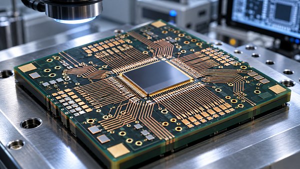
An ABF substrate is a multilayer organic package substrate that uses Ajinomoto Build-up Film as an insulating material in its build-up layers. Along with copper circuitry, a core in many designs, solder mask and other features, these layers create a structure whose components respond differently to heat and mechanical stress.
When temperature changes, each material tends to expand or contract by a different amount. Because the layers are bonded together, they cannot move independently. The resulting mismatch produces internal stresses, and the assembly can bend or twist to accommodate them. Cooling after fabrication or assembly can leave residual stress even when the part returns to room temperature.
The substrate is only one part of that mechanical system. Attaching a silicon die, stiffener, lid, heat spreader or other package component changes the balance of forces. A bare substrate measurement is useful for incoming evaluation, but it does not necessarily predict the shape of the assembled package.
Layer layout also matters. Copper coverage, circuit distribution, dielectric thickness, core construction and asymmetry between the two sides can all influence deformation. Two substrates with the same outer dimensions and nominal thickness can behave differently if their internal stack-ups are different.
Temperature history adds another complication. Polymer materials can change stiffness over the process temperature range, and the response during heating may differ from the response during cooling. A single room-temperature value cannot describe that behavior.
Where warpage disrupts chip assembly
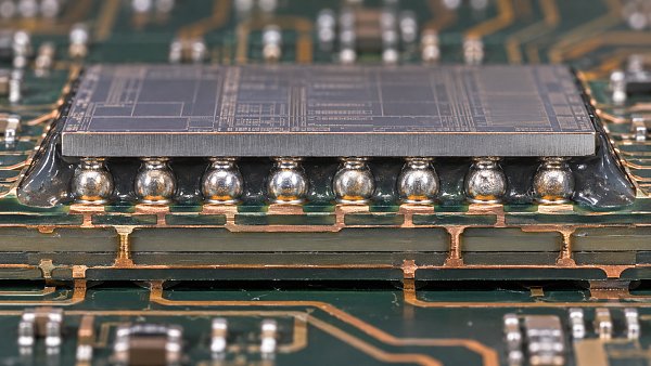
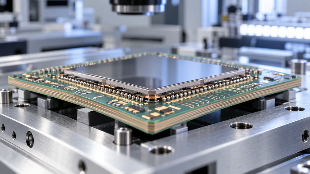
In flip-chip assembly, the die and substrate must be aligned and brought together so that the intended interconnects can form. If the surfaces do not remain sufficiently coplanar at the bonding or reflow temperature, some bumps may make contact while others remain separated. Depending on the interconnect design and process, this can contribute to open connections, non-wet joints, bridging or uneven joint geometry.
Warpage can also affect subsequent package-to-board assembly. A package that deforms during board-level reflow may have an uneven gap relative to the printed circuit board. This can make solder joint formation inconsistent across the package, especially where the package and board deform differently.
The direction of bending is as important as its magnitude. A die and substrate that curve in compatible directions may maintain a more manageable interface than two surfaces that pull apart at the edges or center. The relevant quantity is often the relative gap between mating surfaces, not the maximum warpage of either component considered alone.
Not every defect attributed to warpage is caused by the substrate. Solder volume, surface finish, flux behavior, placement accuracy, temperature uniformity and board deformation can produce similar symptoms or interact with substrate curvature. A useful investigation compares the location and pattern of defects with measured shapes and process conditions before assigning a root cause.
Why a flatness specification alone is not enough
A substrate can pass a room-temperature flatness check and still present a problem at a higher process temperature. It can also behave acceptably during die attach but become more difficult to assemble after additional components have been installed. Acceptance criteria need to reflect the state of the product at the operation where the risk occurs.
For a meaningful comparison, each warpage result should identify:
- Sample configuration: bare substrate, substrate with die, assembled package or package on board.
- Temperature and thermal history: the measurement temperature, heating or cooling direction, and prior thermal cycles where relevant.
- Measurement boundary: the area measured, including whether the reported value covers the whole part or only the assembly region.
- Reference and calculation: how the surface was leveled, the reference plane used, and whether the value represents peak-to-valley displacement or another metric.
- Support condition: how the sample was held and whether the support could restrict its natural deformation.
These details affect whether two numbers describe the same thing. For example, peak-to-valley warpage over an entire substrate can be dominated by an edge outside the die footprint. That measurement may still matter for handling, but it does not fully describe the local gap where bumps must connect.
Sign conventions also need to be explicit. Terms such as “smile” and “cry” can be useful shorthand, but their interpretation depends on viewing direction and the surface being measured. A diagram or an agreed coordinate system is less ambiguous than a label alone.
Measuring warpage across the process window
Optical methods are commonly used to map package or substrate shape without mechanically probing the surface. Depending on the equipment and sample, techniques such as shadow moiré or digital image correlation can provide temperature-dependent deformation information. The choice depends on surface visibility, measurement area, resolution, temperature capability and the type of structure being evaluated.
A temperature profile is generally more informative than a single hot measurement. It can reveal where curvature increases, reverses direction or differs between heating and cooling. Those changes matter because assembly processes include ramps, peak temperatures and cooling, not just one steady condition.
Measurement conditions should resemble the relevant manufacturing step as closely as practical, while acknowledging what the test does and does not reproduce. A free-standing sample in a metrology system may deform differently from a part constrained by a carrier, vacuum chuck or tooling during production. Likewise, a laboratory heating profile may not reproduce the temperature distribution across a production assembly.
Sampling should capture variation across lots and locations on the substrate, as well as variation between individual parts. An average curve can conceal a tail of parts that exceed the process window. For a large panel or strip, the position from which a unit is taken may also matter if processing and material distribution vary across the panel.
Simulation can help interpret these measurements and compare design changes before a full build. Its value depends on representative material properties, layer geometry, manufacturing history and boundary conditions. A model calibrated only against room-temperature shape may not predict high-temperature behavior well enough for process decisions.
Connecting warpage limits to qualification
There is no single warpage number that establishes acceptability for every ABF substrate. The allowable shape depends on the die size, interconnect pitch and geometry, solder or bonding process, package construction, tooling and downstream board assembly. A limit is most useful when it is linked to a known failure mechanism and the process conditions under which that failure can occur.
For a new package or supplier, the evaluation can begin with the critical interfaces: die to substrate, and package to board if board-level assembly is within scope. Define where separation or nonuniform contact would be most damaging, then measure both mating structures under the relevant thermal conditions. Use the resulting shape data to establish the expected relative gap and compare it with what the selected assembly process can accommodate.
Qualification then needs evidence from actual assembly, not metrology alone. Correlate warpage distributions with inspection results, electrical continuity and relevant reliability testing. Include the intended material set and process sequence, because changing a lid, underfill, stiffener or thermal profile can change the stress state and invalidate a comparison based on the bare substrate.
When reviewing supplier data, ask for distributions and test conditions alongside any headline maximum. A reported improvement is difficult to interpret if it comes from a different sample construction, temperature, support fixture or calculation method. Consistency across production lots matters as well as the performance of development samples.
Reducing warpage involves trade-offs
Design changes can reduce deformation by adjusting stack-up symmetry, material selection, copper distribution, substrate thickness or mechanical reinforcement. Their suitability depends on the package. A stiffer construction may improve handling or flatness at one step while changing stress elsewhere, increasing thickness or affecting routing and thermal behavior.
Process changes offer another route. Tooling, temporary support, bonding conditions and thermal profiles can influence how much deformation is present when connections form. These measures may improve assembly robustness without redesigning the substrate, but they also need evaluation for compatibility with throughput, handling and the rest of the process.
Underfill and other encapsulants can redistribute stresses after attachment and support interconnect reliability. They do not automatically correct poor alignment or open joints formed earlier, and their curing and cooling behavior can themselves affect package deformation. They should be treated as part of the package mechanics, not as a substitute for controlling the initial bond.
The strongest decision is therefore made at the package level: agree on the critical temperature-dependent shapes, establish how they relate to assembly defects, and qualify the combined design and process. A flatter substrate can be helpful, but a controlled, repeatable shape that the full assembly process can accommodate is the more useful target.
Questions about market trends? Contact Market Scope Live for deeper business insights.
We respect your privacy. Your information is strictly confidential.
We respect your privacy. Your information is strictly confidential.
Related News
 Advanced PackagingHow accurate do die bonders need to be for flip-chip assembly?Die Bonders for flip-chip assembly must meet post-bond alignment targets. Explore accuracy budgets, process factors and practical tips for choosing the right machine.MORE+
 Advanced PackagingWhen does system-in-package make sense for compact devices?System-in-Package can unlock space and performance in compact devices. Explore the thermal, cost, yield, and supply trade-offs before choosing SiP.MORE+
 Advanced PackagingHow to choose wire bonding equipment for fine-pitch devicesChoose Wire Bonding Equipment for fine-pitch devices with confidence. Compare placement accuracy, bond quality, throughput, supplier trials and ownership costs.MORE+
 Advanced PackagingWhy does ABF substrate warpage matter during chip assembly?ABF Substrates can warp during chip assembly, putting yield and reliability at risk. Discover how to measure deformation and control defects.MORE+
 Advanced PackagingHow Much Floor Space Does a Wire Bonding Machine Need?How much floor space does a wire bonding machine need? Explore footprint, access, utilities, and layout planning to make a confident equipment decision.MORE+
 Advanced PackagingCan a Die Bonder Handle Warped Wafers?How do I check whether a die bonder can handle warped wafers? Compare measurement methods, review process limits, and verify performance with representative wafers.MORE+
 Advanced PackagingWhen do semiconductor packaging substrates need finer line widths?When do Semiconductor Packaging Substrates need finer lines? Explore routing bottlenecks, electrical trade-offs, and supplier checks to make a confident design decision.MORE+
 Advanced PackagingHow underfill materials reduce thermal fatigue in flip-chip packagesDiscover how Semiconductor Underfill Materials reduce flip-chip thermal fatigue, and learn what to consider when selecting and qualifying a formulation.MORE+