When does system-in-package make sense for compact devices?
Author
Date Published
Reading Time
System-in-Package (SiP) makes sense for a compact device when combining several components inside one package saves usable product volume or improves a critical interconnect without creating unacceptable thermal, test, supply, or cost constraints. The strongest case is not simply that the package is smaller than a collection of individual parts. It is that the complete device can meet its requirements more effectively after assembly, qualification, and production losses are considered.
A discrete design remains attractive when the board has sufficient space, components need frequent replacement, heat must be spread across a larger area, or product volumes do not justify custom integration. The decision therefore starts with a constrained device design, not with an assumption that higher integration is inherently better.
Where SiP can solve a real space problem
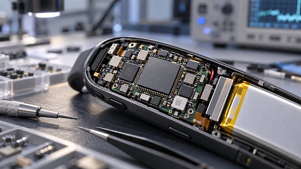
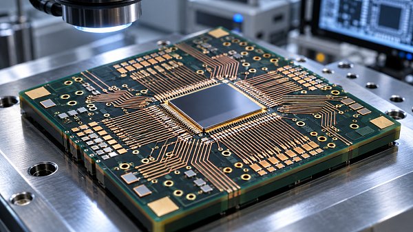
An SiP combines multiple components within a single package to perform a system-level function. Depending on the design, these components can include different semiconductor dies, passive components, and sometimes other elements. The package may use side-by-side placement, stacking, or a combination of approaches. It is distinct from a system-on-chip, which integrates functions on a single die, although an SiP can contain one or more system-on-chip devices.
The relevant comparison is the space occupied by the complete implementation. A discrete design needs room not only for component bodies but also for routing, spacing, power distribution, shielding, assembly tolerances, and sometimes dedicated board layers. An SiP can move some of those connections into the package and release board area for a battery, antenna, sensor placement, or mechanical features.
That benefit is most valuable when a particular board region is genuinely constrained. A wearable, for example, may have a narrow electronics cavity and limited flexibility to move components. Integrating processing, memory, and selected passive components could reduce the area required by the electronic assembly. But if the resulting package is too tall for the enclosure, requires a large keep-out area, or forces a thicker board, its apparent footprint advantage may not translate into a smaller product.
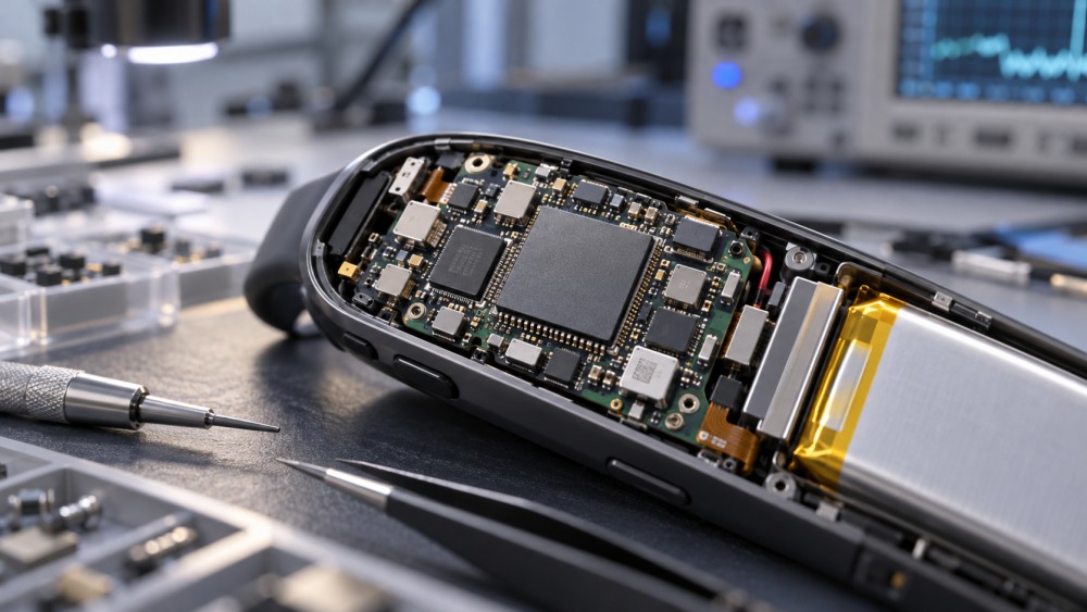
Compare both alternatives using the same enclosure, connectors, antenna requirements, and manufacturing rules. Measure the package and its required board infrastructure together, including any heat-spreading material. A smaller package outline alone is not a sufficient basis for selection.
Shorter connections help only when the interfaces are designed as a system
Bringing dies closer together can reduce interconnect length and associated parasitic effects. That may help a memory interface, a high-speed link, or a sensitive analog path meet performance or power targets. It can also reduce the number of long, externally routed connections on the board.
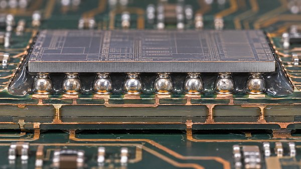
The benefit depends on the actual electrical path. Package substrate traces, redistribution layers, bumps, bond wires, and transitions to the board all contribute resistance, inductance, and capacitance. A shorter nominal distance does not guarantee better signal integrity if the return path is interrupted or package coupling introduces noise.
Power delivery deserves particular attention. A compact package may concentrate current demand into a small area while leaving limited space for decoupling. The design needs an appropriate power-distribution network across the dies, package, and board, with analysis of voltage drop, transient response, and the location and value of decoupling capacitors. Some passives may fit inside the package; others may still need to sit close by on the board.
Radio-frequency and mixed-signal functions introduce another constraint. Placing a radio, processor, memory, and power circuitry close together can save space, but it also creates coupling paths. Shielding, ground structure, clock noise, and package materials influence performance. The antenna remains part of the complete device: integrating the radio does not eliminate the need to validate antenna placement and performance in the final enclosure.
Thermal limits can overturn the footprint advantage
An SiP can concentrate heat from several active components in a smaller area. Stacking can further complicate heat removal because one die may sit between another heat source and the available thermal path. A discrete layout may occupy more board area but allow hot components to be separated and connected to larger copper regions.
The relevant question is not just total package power. It is where heat is generated, how simultaneous operating modes overlap, and how heat leaves the package in the finished product. A sensor node that transmits briefly and sleeps for long periods has a different thermal profile from a compact device that processes data continuously. Peak junction temperatures, transient heating, enclosure temperature, and ambient conditions all matter.
Thermal analysis should represent the proposed die arrangement and the actual product stack-up, including board copper, interface materials, shielding, enclosure contacts, and any restrictions on airflow. Supplier thermal data can inform the model, but a value measured under a different board or test condition should not be treated as the device’s final operating temperature.
If the thermal path requires a heat spreader, thicker board, or larger enclosure, those additions belong in the space and cost comparison. An SiP may still be viable, but its value then depends on whether the other benefits outweigh the lost integration advantage.
Component compatibility and design ownership matter early
Combining components is not simply a matter of placing known parts into one outline. Each die must be available in a form suitable for the chosen assembly process, and its electrical, mechanical, and thermal requirements must be compatible with the rest of the package. Die thickness, pad arrangement, bonding method, operating voltage, and thermal expansion behavior can all affect the design.
Access to bare die is an important practical constraint. A component available as a standard packaged part may not be commercially available as bare die for the intended product, or its supplier may impose handling, test, or supply conditions. The assembly provider also needs the process capability to handle the selected combination. A concept that works on paper can stall if any critical component cannot be sourced and qualified in the required form.
Responsibilities must be explicit across chip suppliers, package designers, assembly providers, and the device maker. Someone must own the combined electrical and thermal specifications, the interfaces between suppliers, and the disposition of failures that cross component boundaries. Without that ownership, an issue at the interface between die and package can become difficult to diagnose or resolve.
Change control is equally consequential. A revision to one die, a substrate material, or an assembly location may require assessment of the entire package and possibly the end product. In a discrete design, changing one component can also trigger qualification, but the affected boundary may be easier to isolate. The right comparison is the expected effort for the specific change, not an assumption that either architecture is always simpler to maintain.
Test coverage and yield determine whether integration scales
SiP cost is influenced by the condition of components before assembly and by what can be tested after they are integrated. If a defective die is assembled with otherwise good components, the resulting package may have to be discarded or reworked. Testing dies before assembly reduces that exposure, but pre-assembly testing may not detect every failure or reproduce every condition encountered in the completed package.
Access also changes after integration. Internal signals that were available at separate component pins may no longer be accessible from the outside. The package may therefore need test features, built-in self-test, suitable probing arrangements, or a way to exercise interfaces through the package’s external connections. These provisions consume design effort and can affect pin count and layout.
Yield must be discussed at defined stages: incoming die test, package assembly, final package test, board assembly, and finished-product test. A single quoted yield cannot explain where losses occur or whether the same failure is counted more than once. For comparison, model the number and cost of good finished assemblies produced from the required inputs, including scrap and any feasible rework at each stage.
Failure analysis is part of the decision. When an integrated module fails in the field, identifying whether the cause lies in a die, an internal connection, the package, or the board can be more difficult than replacing and testing separate components. Agree on diagnostic access, sample handling, reporting, and corrective-action responsibilities before committing to the architecture.
When does the economics justify a custom package?
A custom SiP may reduce board area, component placement operations, or the need for certain external connections. Against those savings are package design and tooling, engineering work, test development, qualification, supplier setup, and the cost of yield losses. The package unit price alone captures neither side of the comparison.
A useful model separates one-time development costs from recurring costs per good finished device. It should include the package, components, assembly, test, substrate, board, rework or scrap, and any mechanical or thermal additions. The discrete alternative should use the same treatment, including its board size, component placement, test, and yield assumptions.
Production volume and product life affect whether the initial investment can be recovered. A reusable module across several products can improve the case, provided the products genuinely share the same requirements and can accept a common change schedule. Conversely, a product that needs frequent component substitutions or uncertain future volumes may benefit from the flexibility of discrete parts, even if its board is larger.
Time to production also belongs in the comparison. A packaged module that already meets the required performance and qualification conditions may offer a different risk profile from a new custom SiP. A prototype demonstrates a design concept; it does not by itself establish stable yield, qualified materials, or sustained supply.
How to judge readiness for the intended device
Before committing to an SiP, define the operating envelope and compare it with evidence for the exact package construction and components under consideration. Qualification of a similar package is useful background, but it does not automatically cover a different die stack, substrate, operating temperature, or end-use environment.
Evidence should connect electrical performance, thermal behavior, mechanical reliability, and manufacturing results. Depending on the product, that can include temperature cycling, humidity exposure, board-level mechanical loading, drop or vibration assessment, and long-duration operation. The test conditions, sample sizes, acceptance criteria, and failure analysis matter as much as a statement that a package has passed qualification.
Supply readiness requires a similarly specific assessment. Confirm who supplies each die and substrate, where assembly and test occur, what capacity is available for the intended schedule, and how changes are communicated. A second source for a discrete component does not necessarily translate into an interchangeable source for a custom integrated package.
The decisive case for SiP is a device in which integration solves a measurable constraint and the complete design remains testable, thermally sound, manufacturable, and supportable. If the space saving disappears after routing, cooling, and reliability requirements are included—or if the package depends on unavailable components or unproven production capability—the discrete alternative is the more credible starting point.
Questions about market trends? Contact Market Scope Live for deeper business insights.
We respect your privacy. Your information is strictly confidential.
We respect your privacy. Your information is strictly confidential.
Related News
 Advanced PackagingHow accurate do die bonders need to be for flip-chip assembly?Die Bonders for flip-chip assembly must meet post-bond alignment targets. Explore accuracy budgets, process factors and practical tips for choosing the right machine.MORE+
 Advanced PackagingWhen does system-in-package make sense for compact devices?System-in-Package can unlock space and performance in compact devices. Explore the thermal, cost, yield, and supply trade-offs before choosing SiP.MORE+
 Advanced PackagingHow to choose wire bonding equipment for fine-pitch devicesChoose Wire Bonding Equipment for fine-pitch devices with confidence. Compare placement accuracy, bond quality, throughput, supplier trials and ownership costs.MORE+
 Advanced PackagingWhy does ABF substrate warpage matter during chip assembly?ABF Substrates can warp during chip assembly, putting yield and reliability at risk. Discover how to measure deformation and control defects.MORE+
 Advanced PackagingHow Much Floor Space Does a Wire Bonding Machine Need?How much floor space does a wire bonding machine need? Explore footprint, access, utilities, and layout planning to make a confident equipment decision.MORE+
 Advanced PackagingCan a Die Bonder Handle Warped Wafers?How do I check whether a die bonder can handle warped wafers? Compare measurement methods, review process limits, and verify performance with representative wafers.MORE+
 Advanced PackagingWhen do semiconductor packaging substrates need finer line widths?When do Semiconductor Packaging Substrates need finer lines? Explore routing bottlenecks, electrical trade-offs, and supplier checks to make a confident design decision.MORE+
 Advanced PackagingHow underfill materials reduce thermal fatigue in flip-chip packagesDiscover how Semiconductor Underfill Materials reduce flip-chip thermal fatigue, and learn what to consider when selecting and qualifying a formulation.MORE+